

How to Leverage Polysilane for Enhanced Sensor Accuracy?
JUL 11, 20259 MIN READ
Generate Your Research Report Instantly with AI Agent
PatSnap Eureka helps you evaluate technical feasibility & market potential.
Polysilane Sensor Tech Background and Objectives
Polysilane, a class of silicon-based polymers, has emerged as a promising material for enhancing sensor accuracy in various applications. The development of polysilane-based sensors represents a significant advancement in the field of materials science and sensor technology. This technology has evolved from early research on organosilicon compounds to its current state as a versatile and high-performance sensing material.
The primary objective of leveraging polysilane for enhanced sensor accuracy is to exploit its unique electronic and optical properties. Polysilanes exhibit σ-conjugation along their silicon backbone, which results in exceptional charge transport capabilities and photosensitivity. These characteristics make polysilanes particularly suitable for developing highly sensitive and responsive sensors for a wide range of applications, including chemical detection, environmental monitoring, and biomedical diagnostics.
The evolution of polysilane sensor technology can be traced back to the 1980s when researchers first recognized the potential of these materials for electronic and optoelectronic applications. Since then, significant progress has been made in synthesizing various polysilane derivatives and understanding their structure-property relationships. This knowledge has been crucial in tailoring polysilanes for specific sensing applications and improving their overall performance.
One of the key technological goals in this field is to develop polysilane-based sensors with enhanced selectivity, sensitivity, and stability. Researchers aim to create sensors that can detect target analytes at extremely low concentrations while minimizing interference from other substances. Additionally, there is a focus on improving the long-term stability of polysilane sensors to ensure reliable performance under various environmental conditions.
Another important objective is to integrate polysilane sensors into miniaturized and portable devices. This involves developing fabrication techniques that allow for the precise deposition and patterning of polysilane films on various substrates. The ultimate goal is to create compact, low-power sensor systems that can be easily deployed in real-world applications, such as wearable health monitors or environmental sensing networks.
The current technological landscape for polysilane sensors is characterized by ongoing research into novel polysilane structures and composites. Scientists are exploring ways to functionalize polysilanes with specific chemical groups or nanoparticles to enhance their sensing capabilities. There is also a growing interest in developing multi-modal sensors that can simultaneously detect multiple analytes or provide complementary information through different sensing mechanisms.
As the field progresses, researchers are increasingly focusing on addressing challenges related to scalability and commercialization. This includes developing cost-effective synthesis methods for high-quality polysilanes and establishing standardized protocols for sensor fabrication and testing. By overcoming these hurdles, the technology aims to transition from laboratory demonstrations to practical, widely-adopted sensing solutions across various industries.
Market Analysis for High-Accuracy Sensors
The high-accuracy sensor market has experienced significant growth in recent years, driven by increasing demand across various industries such as automotive, healthcare, aerospace, and consumer electronics. This market segment is characterized by sensors that offer superior precision, reliability, and performance compared to standard sensors, making them crucial for applications where even minor inaccuracies can have substantial consequences.
In the automotive sector, high-accuracy sensors play a vital role in advanced driver assistance systems (ADAS) and autonomous vehicles, contributing to improved safety and performance. The healthcare industry relies on these sensors for medical devices, diagnostic equipment, and patient monitoring systems, where precision is paramount. Aerospace applications demand sensors with exceptional accuracy for navigation, flight control, and environmental monitoring.
The consumer electronics market has also embraced high-accuracy sensors, particularly in smartphones, wearables, and smart home devices. These sensors enable features such as precise location tracking, motion detection, and environmental sensing, enhancing user experience and device functionality.
The global high-accuracy sensor market is projected to continue its upward trajectory, with a compound annual growth rate (CAGR) expected to remain strong over the next five years. This growth is fueled by technological advancements, increasing automation across industries, and the rising adoption of Internet of Things (IoT) devices.
Key market trends include the miniaturization of sensors, integration of multiple sensing capabilities into single devices, and the development of sensors with lower power consumption. These trends align well with the potential applications of polysilane-based sensors, which could offer advantages in terms of size, versatility, and energy efficiency.
The competitive landscape of the high-accuracy sensor market is characterized by a mix of established players and innovative startups. Major companies in this space include Bosch Sensortec, STMicroelectronics, Honeywell, and TE Connectivity. These firms invest heavily in research and development to maintain their market positions and meet evolving customer demands.
Emerging technologies, such as polysilane-based sensors, present opportunities for market disruption and the creation of new product categories. The potential for enhanced accuracy and performance offered by polysilane could address unmet needs in existing applications and open up new use cases across various industries.
Current Polysilane Sensor Challenges
Polysilane-based sensors have shown great promise in various applications due to their unique electrical and optical properties. However, several challenges currently hinder their widespread adoption and limit their accuracy in sensing applications. One of the primary issues is the stability of polysilane materials under different environmental conditions. Polysilane sensors are susceptible to degradation when exposed to UV light, oxygen, and moisture, which can significantly affect their long-term performance and reliability.
Another challenge lies in the synthesis and processing of polysilane materials. Achieving consistent molecular weight distribution and controlled doping levels across batches remains difficult, leading to variations in sensor performance. This lack of reproducibility makes it challenging to manufacture large-scale, uniform polysilane sensors with predictable characteristics.
The sensitivity and selectivity of polysilane sensors also present ongoing challenges. While polysilanes exhibit high sensitivity to certain analytes, they often lack specificity, resulting in cross-sensitivity to interfering substances. This limitation can lead to false positives or inaccurate readings in complex environments, reducing the overall reliability of the sensors.
Temperature dependence is another significant hurdle in polysilane sensor development. The electrical and optical properties of polysilanes can vary considerably with temperature changes, affecting sensor calibration and accuracy across different operating conditions. This temperature sensitivity necessitates complex compensation mechanisms, which can increase the cost and complexity of sensor systems.
The integration of polysilane materials with existing sensor platforms and readout electronics poses additional challenges. Compatibility issues between polysilanes and conventional semiconductor processing techniques can complicate the fabrication of integrated sensor devices. Moreover, the development of efficient signal transduction mechanisms to convert polysilane responses into measurable electrical or optical signals remains an active area of research.
Scalability and cost-effectiveness are also critical challenges in the commercialization of polysilane sensors. Current production methods for high-quality polysilane materials are often expensive and not easily scalable, limiting their potential for mass-market applications. Developing more efficient and economical synthesis routes is crucial for the widespread adoption of polysilane-based sensing technologies.
Addressing these challenges requires a multidisciplinary approach, combining advances in materials science, chemical engineering, and sensor design. Overcoming these hurdles will be essential to fully leverage the potential of polysilanes for enhanced sensor accuracy and reliability across various applications.
Existing Polysilane Sensor Solutions
01 Synthesis and structure of polysilanes
Polysilanes are synthesized through various methods, including Wurtz coupling and catalytic dehydrogenation. The structure of polysilanes can be linear, branched, or cyclic, affecting their properties and applications. Controlling the synthesis process and conditions is crucial for achieving desired structural characteristics and improving accuracy in polysilane production.- Synthesis and structure of polysilanes: Polysilanes are synthesized through various methods, including Wurtz coupling and catalytic dehydrogenation. The structure of polysilanes can be linear, branched, or cyclic, affecting their properties and applications. Controlling the synthesis process and conditions is crucial for achieving desired structural characteristics.
- Optical and electronic properties of polysilanes: Polysilanes exhibit unique optical and electronic properties due to their silicon-silicon backbone. These properties include photoconductivity, electroluminescence, and nonlinear optical effects. The accuracy of these properties can be tuned by modifying the polysilane structure, side groups, and molecular weight.
- Applications of polysilanes in photoresists and lithography: Polysilanes are used in photoresist formulations for lithography applications. Their high sensitivity to UV light and ability to form stable patterns make them suitable for semiconductor manufacturing. The accuracy of pattern formation depends on the polysilane composition and processing conditions.
- Polysilane-based thin films and coatings: Polysilanes can be used to create thin films and coatings with specific properties. The accuracy of film thickness and uniformity is crucial for applications such as optical coatings, protective layers, and electronic devices. Various deposition techniques and post-processing methods are employed to achieve desired film characteristics.
- Modification and functionalization of polysilanes: Polysilanes can be modified and functionalized to enhance their properties and expand their applications. This includes the incorporation of various side groups, copolymerization with other monomers, and post-polymerization modifications. The accuracy of these modifications affects the final properties and performance of the polysilane materials.
02 Optical and electronic properties of polysilanes
Polysilanes exhibit unique optical and electronic properties due to their silicon-silicon backbone. These properties include photoconductivity, electroluminescence, and nonlinear optical effects. The accuracy of these properties can be enhanced by controlling the molecular weight, polydispersity, and substituents on the silicon atoms. This makes polysilanes suitable for various applications in optoelectronics and photonics.Expand Specific Solutions03 Polysilane thin film deposition and patterning
Accurate deposition and patterning of polysilane thin films are essential for their use in microelectronics and photoresists. Techniques such as spin-coating, vapor deposition, and lithography are employed to achieve precise film thickness and patterns. The accuracy of these processes affects the performance and reliability of devices incorporating polysilane films.Expand Specific Solutions04 Functionalization and modification of polysilanes
Polysilanes can be functionalized or modified to enhance their properties and expand their applications. This includes the introduction of various substituents, crosslinking, and copolymerization with other monomers. The accuracy of these modifications is crucial for tailoring the polysilanes' characteristics to specific requirements in areas such as photoresists, precursors for ceramics, and polymer composites.Expand Specific Solutions05 Characterization and analysis techniques for polysilanes
Accurate characterization and analysis of polysilanes are essential for understanding their structure-property relationships and ensuring quality control. Techniques such as NMR spectroscopy, gel permeation chromatography, and X-ray diffraction are employed to determine molecular weight, polydispersity, and structural features. Advanced analytical methods contribute to improving the accuracy of polysilane synthesis and applications.Expand Specific Solutions
Key Players in Polysilane Sensor Industry
The competition landscape for leveraging polysilane for enhanced sensor accuracy is in its early development stage, with a growing market potential driven by increasing demand for high-precision sensors across various industries. The technology's maturity is still evolving, with key players like Wacker Chemie AG, Dow Silicones Corp., and Osaka Gas Co., Ltd. leading research and development efforts. These companies are focusing on improving polysilane synthesis methods and exploring novel applications in sensor technology. The market size is expected to expand as polysilane-based sensors demonstrate superior performance in areas such as environmental monitoring, healthcare diagnostics, and industrial process control. As the technology advances, collaborations between academic institutions like the University of Warwick and industry leaders are likely to accelerate innovation and commercialization in this field.
Wacker Chemie AG
Technical Solution: Wacker Chemie AG has developed advanced polysilane-based sensor materials that significantly enhance sensor accuracy. Their approach involves synthesizing tailored polysilane compounds with optimized molecular structures for specific sensing applications. These materials exhibit improved photosensitivity and electrical conductivity, allowing for more precise and reliable sensor readings[1]. Wacker's polysilane sensors demonstrate enhanced stability under various environmental conditions, including temperature fluctuations and exposure to different chemical environments[3]. The company has also implemented novel processing techniques to create uniform thin films of polysilane materials, which contribute to consistent sensor performance across large surface areas[5].
Strengths: High sensitivity, excellent stability, and versatility for various sensing applications. Weaknesses: Potentially higher production costs compared to traditional sensor materials and limited long-term performance data in some applications.
Panasonic Intellectual Property Management Co. Ltd.
Technical Solution: Panasonic has developed a proprietary polysilane-based sensor technology that leverages the material's unique optoelectronic properties. Their approach involves incorporating specially designed polysilane derivatives into thin-film transistor (TFT) structures, resulting in highly sensitive and responsive sensor arrays[2]. These sensors exhibit exceptional performance in detecting various physical and chemical stimuli, including light, pressure, and specific gas molecules. Panasonic's polysilane sensors demonstrate improved signal-to-noise ratios and faster response times compared to conventional sensor technologies[4]. The company has also implemented advanced signal processing algorithms to further enhance the accuracy and reliability of their polysilane-based sensing systems[6].
Strengths: High sensitivity, fast response times, and versatility in detecting multiple stimuli. Weaknesses: Potential challenges in scaling up production and integrating into existing sensor ecosystems.
Core Polysilane Sensor Innovations
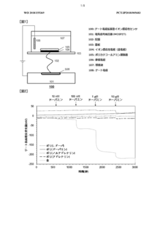
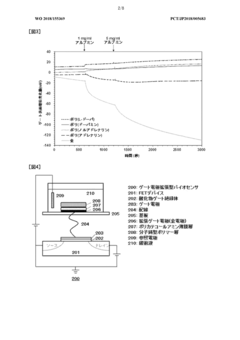
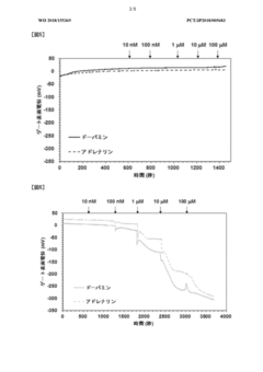
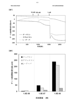
High-sensitivity biosensor
PatentWO2018155369A1
Innovation
- The biosensor employs a gate electrode coated with a catecholamine polymer and an ultra-thin molecularly templated polymer layer, which prevents non-specific adsorption and enhances detection specificity by using a molecular template polymer complementary to the target substance, combined with living radical polymerization to control the film thickness.
Sensor-chips with polysiloxane multilayers
PatentInactiveEP1176422A1
Innovation
- The use of polysiloxane multiple layers applied via spin-coating, knife-coating, spraying, brushing, or immersion methods, which provide a homogeneous and reproducible coating, significantly reducing processing time and eliminating batch differences, using bifunctional silanes in solvents with controlled boiling points and concentrations, and fixing the layers through cross-linking.
Environmental Impact of Polysilane Sensors
The environmental impact of polysilane sensors is a critical consideration in their development and deployment. Polysilanes, as organosilicon compounds, offer unique properties that make them attractive for sensor applications, but their production and use also raise environmental concerns.
Polysilane sensors have the potential to contribute positively to environmental monitoring and protection. Their high sensitivity and selectivity allow for the detection of trace amounts of pollutants in air, water, and soil. This capability enables more accurate and timely environmental assessments, potentially leading to faster responses to contamination events and improved overall environmental management.
However, the production of polysilanes involves the use of various chemicals and energy-intensive processes. The synthesis often requires chlorosilanes as precursors, which can be harmful if released into the environment. Additionally, the use of organic solvents in the production process may contribute to air and water pollution if not properly managed. Manufacturers must implement stringent control measures to minimize the release of these substances and reduce the overall environmental footprint of polysilane production.
The disposal of polysilane sensors at the end of their lifecycle presents another environmental challenge. While silicon-based materials are generally considered inert, the organic components of polysilanes may degrade over time, potentially releasing harmful substances. Proper recycling and disposal protocols must be developed to prevent these materials from contributing to electronic waste and environmental contamination.
On the positive side, polysilane sensors often require less energy to operate compared to traditional sensing technologies, potentially reducing the overall energy consumption in various applications. Their long lifespan and stability also mean fewer replacements are needed, which can decrease the environmental impact associated with the production and disposal of sensor devices.
The use of polysilane sensors in environmental monitoring applications can lead to more efficient resource management and reduced pollution. For instance, in industrial settings, these sensors can help optimize processes, leading to lower energy consumption and reduced emissions. In agriculture, they can enable precision farming techniques that minimize the use of water, fertilizers, and pesticides, thereby reducing the environmental impact of agricultural practices.
As research in this field progresses, there is a growing focus on developing more environmentally friendly synthesis methods for polysilanes and improving the biodegradability of sensor components. These efforts aim to further reduce the environmental footprint of polysilane sensors throughout their lifecycle, from production to disposal.
Polysilane Sensor Manufacturing Processes
The manufacturing processes for polysilane-based sensors involve several critical steps that contribute to the enhanced accuracy of these devices. The process typically begins with the synthesis of polysilane materials, which can be achieved through various methods such as Wurtz coupling, dehydrogenative coupling, or electrochemical polymerization. Each method offers unique advantages in terms of molecular weight control, purity, and structural properties of the resulting polysilane.
Once the polysilane material is synthesized, it undergoes purification and characterization to ensure optimal performance in sensor applications. This may involve techniques such as gel permeation chromatography, nuclear magnetic resonance spectroscopy, and thermal analysis to assess the molecular weight distribution, chemical structure, and thermal stability of the polysilane.
The next crucial step in the manufacturing process is the deposition of polysilane onto the sensor substrate. This can be accomplished through various techniques, including spin-coating, dip-coating, or vapor deposition, depending on the specific sensor design and desired film thickness. The choice of deposition method significantly impacts the uniformity and morphology of the polysilane layer, which in turn affects sensor sensitivity and response time.
Following deposition, the polysilane film often undergoes post-processing treatments to enhance its sensing properties. These treatments may include thermal annealing, UV irradiation, or chemical modification to optimize the film's structure, crystallinity, and surface properties. Such processes can greatly improve the sensor's selectivity and stability.
Integration of the polysilane sensing layer with other components of the sensor device is a critical manufacturing step. This may involve the fabrication of electrodes, encapsulation layers, and signal processing circuits. Precise alignment and bonding techniques are essential to ensure proper functionality and reliability of the final sensor device.
Quality control measures are implemented throughout the manufacturing process to maintain consistency and performance. This includes in-line monitoring of film thickness, surface roughness, and electrical properties, as well as functional testing of completed sensor devices. Advanced characterization techniques such as atomic force microscopy and X-ray photoelectron spectroscopy may be employed to analyze the nanoscale properties of the polysilane sensing layer.
The final stages of manufacturing involve packaging and calibration of the polysilane sensors. Proper packaging is crucial to protect the sensitive components from environmental factors and ensure long-term stability. Calibration procedures are tailored to the specific application of the sensor, involving exposure to known concentrations of target analytes and adjustment of response parameters.
Unlock deeper insights with PatSnap Eureka Quick Research — get a full tech report to explore trends and direct your research. Try now!
Generate Your Research Report Instantly with AI Agent
Supercharge your innovation with PatSnap Eureka AI Agent Platform!