Innovations in AMOLED backplane technologies.
JUL 17, 20259 MIN READ
Generate Your Research Report Instantly with AI Agent
Patsnap Eureka helps you evaluate technical feasibility & market potential.
AMOLED Backplane Evolution
The evolution of AMOLED backplane technologies has been a critical factor in the advancement of display technology. Initially, amorphous silicon (a-Si) was the dominant material used in thin-film transistors (TFTs) for AMOLED displays. However, its limitations in electron mobility and stability led to the exploration of alternative materials.
Low-temperature polycrystalline silicon (LTPS) emerged as a significant improvement, offering higher electron mobility and better stability. This allowed for smaller TFTs and higher pixel densities, enabling the production of high-resolution AMOLED displays. LTPS technology became widely adopted in the industry, particularly for high-end smartphones and tablets.
As demand for larger AMOLED displays grew, the industry faced challenges with LTPS due to its complex manufacturing process and high production costs. This led to the development of oxide semiconductor materials, particularly indium gallium zinc oxide (IGZO). IGZO offered a balance between performance and cost-effectiveness, making it suitable for larger displays and enabling the expansion of AMOLED technology into televisions and monitors.
Recent years have seen further innovations in backplane technologies. The introduction of low-temperature polycrystalline oxide (LTPO) has combined the benefits of LTPS and oxide semiconductors. LTPO allows for variable refresh rates, significantly improving power efficiency in mobile devices.
Advancements in quantum dot technology have also influenced backplane development. Quantum dot color conversion layers integrated with AMOLED backplanes have enabled wider color gamuts and improved color accuracy.
The ongoing research in flexible and stretchable electronics has pushed the boundaries of backplane technology. New materials and fabrication techniques are being explored to create bendable and foldable AMOLED displays, opening up possibilities for innovative device form factors.
Looking towards the future, there is significant interest in developing ultra-thin and transparent backplanes. These could enable the integration of AMOLED displays into a wider range of products, including augmented reality glasses and smart windows.
The evolution of AMOLED backplane technologies continues to drive improvements in display performance, energy efficiency, and form factor flexibility. As research progresses, we can expect further innovations that will shape the future of display technology and its applications across various industries.
Display Market Trends
The display market has been experiencing significant shifts in recent years, driven by technological advancements and changing consumer preferences. AMOLED (Active-Matrix Organic Light-Emitting Diode) technology has emerged as a key player in this evolving landscape, particularly in the mobile device sector. The demand for AMOLED displays has been steadily increasing, with manufacturers recognizing its advantages in terms of picture quality, energy efficiency, and form factor flexibility.
The smartphone market, which has been the primary driver of AMOLED adoption, continues to show strong growth potential. High-end smartphones have been quick to incorporate AMOLED displays, with the technology gradually trickling down to mid-range devices as production costs decrease. This trend is expected to continue, further expanding the market share of AMOLED displays in the mobile sector.
Beyond smartphones, the AMOLED market is diversifying into other product categories. Wearable devices, such as smartwatches and fitness trackers, have been increasingly adopting AMOLED displays due to their power efficiency and vibrant color reproduction. The automotive industry is another emerging market for AMOLED technology, with premium car manufacturers integrating these displays into their infotainment systems and digital dashboards.
The television segment is also witnessing a gradual shift towards AMOLED technology, particularly in the high-end market. While LCD still dominates the overall TV market, AMOLED TVs are gaining traction among consumers seeking superior picture quality and thinner form factors. As production capabilities improve and costs decrease, AMOLED is expected to capture a larger share of the TV market in the coming years.
The display industry is also seeing increased interest in flexible and foldable displays, an area where AMOLED technology excels. The unique properties of OLED materials allow for the creation of bendable and rollable displays, opening up new form factors and use cases. This trend is likely to drive further innovation in AMOLED backplane technologies to support these novel display formats.
As the AMOLED market expands, there is growing pressure on manufacturers to improve production efficiency and yield rates. This has led to increased investment in research and development of advanced backplane technologies. Innovations in this area are crucial for reducing production costs, improving display performance, and enabling new form factors. The industry is exploring various approaches, including the use of new materials and novel transistor designs, to enhance AMOLED backplane capabilities.
AMOLED Tech Challenges
AMOLED displays have revolutionized the mobile device industry with their superior image quality and energy efficiency. However, the technology still faces several significant challenges that hinder its widespread adoption and further advancement. One of the primary issues is the complexity and cost of manufacturing AMOLED backplanes, which require high-precision processes and expensive materials.
The backplane, responsible for driving individual pixels, demands exceptional performance in terms of electron mobility and stability. Current thin-film transistor (TFT) technologies, such as low-temperature polycrystalline silicon (LTPS) and amorphous silicon (a-Si), struggle to meet the increasing demands of higher resolution and refresh rates while maintaining power efficiency. LTPS offers high mobility but suffers from non-uniformity issues across large areas, while a-Si lacks the necessary electron mobility for advanced display applications.
Another significant challenge is the degradation of organic materials used in AMOLED displays. The organic light-emitting diodes are susceptible to oxidation and moisture, leading to reduced lifespan and potential color shifts over time. This necessitates complex encapsulation techniques, which add to the overall cost and manufacturing complexity.
Power consumption remains a concern, particularly for mobile devices where battery life is crucial. While AMOLEDs are generally more energy-efficient than LCDs for displaying dark content, they can consume more power when displaying bright or white images. Balancing power efficiency across various content types is an ongoing challenge for display engineers.
Scaling AMOLED technology to larger screen sizes presents additional hurdles. As display sizes increase, maintaining uniform brightness and color across the entire panel becomes more difficult due to voltage drops and current distribution issues in the backplane circuitry. This challenge is particularly evident in the development of AMOLED televisions and monitors.
The pursuit of higher pixel densities for applications like virtual and augmented reality headsets pushes the limits of current backplane technologies. Achieving the necessary pixel densities while maintaining high refresh rates and low latency requires significant advancements in TFT performance and circuit design.
Lastly, the environmental impact of AMOLED production is a growing concern. The manufacturing process involves hazardous materials and energy-intensive steps, prompting the need for more sustainable production methods and materials. Addressing these environmental challenges is crucial for the long-term viability and acceptance of AMOLED technology in an increasingly eco-conscious market.
Current Backplane Solutions
01 AMOLED backplane structure and fabrication
AMOLED backplanes are crucial components in display technology, consisting of thin-film transistors (TFTs) and other electronic elements. The structure and fabrication process of these backplanes involve various layers and materials to achieve optimal performance. Advanced techniques are employed to create high-quality, efficient backplanes for AMOLED displays.- AMOLED backplane structure: The AMOLED backplane structure typically consists of thin-film transistors (TFTs) arranged in a matrix to control individual pixels. This structure includes various layers such as the substrate, gate electrodes, semiconductor layer, and source/drain electrodes. The design and arrangement of these components are crucial for the performance and efficiency of the AMOLED display.
- Driving circuits for AMOLED displays: Driving circuits are essential components of AMOLED backplanes, responsible for controlling the current flow to each pixel. These circuits often include scan drivers, data drivers, and power management units. Advanced driving schemes are implemented to improve display performance, reduce power consumption, and enhance image quality.
- Pixel circuit design for AMOLED displays: Pixel circuits in AMOLED backplanes are designed to control the current flowing through each OLED pixel. These circuits typically include multiple transistors and capacitors to ensure stable current supply and compensate for variations in TFT characteristics. Advanced pixel circuit designs aim to improve uniformity, reduce power consumption, and enhance display lifetime.
- Manufacturing processes for AMOLED backplanes: The manufacturing of AMOLED backplanes involves various processes such as deposition, photolithography, etching, and annealing. Advanced techniques are employed to improve the quality and yield of TFTs and other components. These processes are crucial for achieving high-performance, large-area, and flexible AMOLED displays.
- Integration of additional functionalities in AMOLED backplanes: AMOLED backplanes can be integrated with additional functionalities to enhance display performance and user experience. These may include touch sensors, fingerprint sensors, or other sensing capabilities embedded within the backplane structure. Such integration can lead to thinner and more compact display modules with advanced features.
02 Pixel circuit design for AMOLED displays
Pixel circuits in AMOLED backplanes are designed to control individual pixels, ensuring uniform brightness and color accuracy. These circuits often include multiple transistors and capacitors to manage current flow and compensate for variations in OLED characteristics. Innovative circuit designs aim to improve display performance and reduce power consumption.Expand Specific Solutions03 Driving methods for AMOLED backplanes
Various driving methods are employed to operate AMOLED backplanes efficiently. These methods include different scanning and data signal application techniques to optimize display quality and reduce power consumption. Advanced driving schemes can compensate for TFT variations and OLED degradation, ensuring consistent performance over time.Expand Specific Solutions04 Integration of sensors in AMOLED backplanes
AMOLED backplanes can be integrated with various sensors, such as touch sensors or fingerprint sensors, to enhance device functionality. This integration often requires careful design considerations to maintain display performance while incorporating additional sensing capabilities. Advanced manufacturing techniques are used to achieve seamless integration of sensors within the backplane structure.Expand Specific Solutions05 Thermal management in AMOLED backplanes
Effective thermal management is crucial for AMOLED backplanes to ensure optimal performance and longevity. Various techniques are employed to dissipate heat generated during operation, including the use of heat-spreading materials and innovative structural designs. Proper thermal management helps maintain consistent display quality and prevents premature degradation of OLED materials.Expand Specific Solutions
AMOLED Industry Leaders
The AMOLED backplane technology market is in a growth phase, driven by increasing demand for high-quality displays in smartphones, TVs, and other electronic devices. The global market size is projected to expand significantly in the coming years, with major players like Samsung Electronics, BOE Technology, and TCL China Star Optoelectronics leading the innovation race. These companies are investing heavily in R&D to improve AMOLED performance, efficiency, and manufacturing processes. The technology's maturity is advancing rapidly, with companies like IGNIS Innovation and Universal Display Corporation developing novel solutions to address challenges such as image sticking and burn-in. As the industry progresses, we can expect to see further advancements in flexible displays, higher resolutions, and enhanced energy efficiency.
BOE Technology Group Co., Ltd.
Technical Solution: BOE has made significant strides in AMOLED backplane technologies, focusing on oxide semiconductor thin-film transistors (TFTs) for high-resolution displays. Their innovative approach includes the development of low-temperature polycrystalline oxide (LTPO) backplanes, which enable variable refresh rates and improved power efficiency[1]. BOE has also introduced advanced compensation circuits to address issues like non-uniform brightness and color shift in AMOLED displays. Their latest generation of flexible AMOLED panels incorporates a unique pixel circuit design that enhances image quality and reduces power consumption by up to 15%[3].
Strengths: Large-scale production capability, advanced R&D in oxide TFTs, and flexible display technologies. Weaknesses: Relatively new entrant in high-end AMOLED market compared to some competitors, potential yield issues with cutting-edge technologies.
Samsung Electronics Co., Ltd.
Technical Solution: Samsung has pioneered several innovations in AMOLED backplane technologies. They have developed and implemented low-temperature polycrystalline silicon (LTPS) TFTs, which offer higher electron mobility and enable higher resolution displays. Samsung's latest breakthrough is the commercialization of quantum dot (QD)-OLED technology, which combines quantum dots with blue OLED emitters to achieve superior color performance and energy efficiency[2]. Their backplane innovations also include advanced pixel circuits that compensate for TFT threshold voltage variations, improving display uniformity. Samsung has reported achieving pixel densities exceeding 1000 PPI in their latest AMOLED displays, suitable for VR applications[4].
Strengths: Market leader in AMOLED production, extensive R&D capabilities, and vertical integration. Weaknesses: High production costs for cutting-edge technologies, potential oversupply risks in the display market.
Key AMOLED Patents
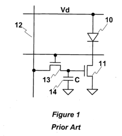
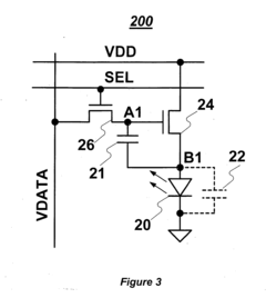
Active matrix organic light emitting diode back plate, method for preparing the same, and display panel
PatentInactiveUS20200335558A1
Innovation
- An active matrix organic light emitting diode back plate is designed with a thin film transistor and a thin film battery integrated coplanarly on a substrate, allowing for a single preparation process and maximizing integration, which reduces module thickness, simplifies the preparation process, and lowers production costs.
Method and system for programming and driving active matrix light emitting device pixel having a controllable supply voltage
PatentActiveUS20150379932A1
Innovation
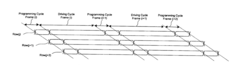
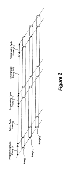
- A method and system for programming and driving AMOLED displays that involves a pixel circuit with a driving transistor, a switch transistor, and storage capacitors, where voltages are controlled during programming cycles to store differences in nodes, allowing the application of a stable gate-source voltage independent of the threshold voltage, thereby maintaining constant current flow through the OLED.
Material Advancements
Material advancements play a crucial role in driving innovations in AMOLED backplane technologies. The continuous evolution of materials used in the fabrication of thin-film transistors (TFTs) and other components has significantly improved the performance and efficiency of AMOLED displays.
One of the most notable advancements in backplane materials is the development of oxide semiconductors, particularly indium gallium zinc oxide (IGZO). IGZO offers superior electron mobility compared to traditional amorphous silicon (a-Si), enabling faster switching speeds and lower power consumption. This material has become increasingly popular in high-resolution displays, as it allows for smaller pixel sizes and improved aperture ratios.
Another promising material for AMOLED backplanes is low-temperature polycrystalline silicon (LTPS). LTPS offers even higher electron mobility than IGZO, making it suitable for ultra-high-resolution displays and high-refresh-rate applications. However, its manufacturing process is more complex and costly, limiting its widespread adoption.
Recent research has focused on developing organic semiconductors for use in AMOLED backplanes. These materials offer the potential for flexible and stretchable displays, as they can be processed at lower temperatures and are inherently more pliable than inorganic semiconductors. Organic TFTs (OTFTs) have shown promising results in terms of flexibility and transparency, although their stability and performance still lag behind their inorganic counterparts.
Advancements in dielectric materials have also contributed to improved AMOLED backplane performance. High-k dielectrics, such as hafnium oxide and aluminum oxide, allow for thinner gate insulators while maintaining low leakage currents. This enables better control of the TFT channel and reduces power consumption.
The development of novel electrode materials has further enhanced AMOLED backplane technologies. Transparent conductive oxides (TCOs) like indium tin oxide (ITO) have been widely used, but researchers are exploring alternatives such as graphene and silver nanowires to improve conductivity and flexibility while reducing costs.
Encapsulation materials have seen significant improvements, addressing one of the primary challenges in AMOLED technology: moisture and oxygen sensitivity. Advanced thin-film encapsulation (TFE) techniques using alternating layers of inorganic and organic materials have greatly enhanced the longevity and reliability of AMOLED displays, particularly in flexible and foldable applications.
These material advancements collectively contribute to the ongoing evolution of AMOLED backplane technologies, enabling higher performance, improved efficiency, and novel form factors in display applications.
Manufacturing Processes
The manufacturing processes for AMOLED backplane technologies have undergone significant advancements in recent years, driven by the demand for higher resolution, improved performance, and cost-effective production methods. One of the key innovations in this area is the development of low-temperature polycrystalline silicon (LTPS) technology, which allows for the creation of high-performance thin-film transistors (TFTs) on flexible substrates.
LTPS manufacturing typically involves the deposition of amorphous silicon on a substrate, followed by laser annealing to crystallize the silicon. This process enables the formation of high-mobility TFTs, which are essential for driving OLED pixels efficiently. The laser annealing step has seen improvements in precision and uniformity, leading to better consistency in device performance across large panel areas.
Another significant advancement is the introduction of oxide semiconductor materials, such as indium gallium zinc oxide (IGZO), for TFT fabrication. IGZO offers several advantages over traditional amorphous silicon, including higher electron mobility and lower off-state current. The manufacturing process for IGZO TFTs typically involves sputtering deposition of the oxide layers, followed by annealing and patterning steps.
Photolithography techniques used in backplane manufacturing have also evolved to accommodate the increasing pixel densities of AMOLED displays. Advanced photoresists and exposure systems allow for finer feature sizes and more precise patterning of TFT structures. Multi-patterning techniques, such as self-aligned double patterning (SADP), have been adopted to achieve sub-micron feature sizes in high-resolution displays.
The integration of copper metallization in AMOLED backplanes has been another important innovation. Copper offers lower resistance compared to traditional aluminum interconnects, enabling faster signal transmission and reduced power consumption. The manufacturing process for copper metallization typically involves damascene techniques, where trenches are etched into dielectric layers and then filled with copper using electroplating methods.
Encapsulation processes have also seen significant improvements to enhance the longevity and reliability of AMOLED displays. Thin-film encapsulation (TFE) technologies, such as atomic layer deposition (ALD) of barrier layers, provide effective protection against moisture and oxygen ingress. These processes allow for the creation of flexible and foldable AMOLED displays by eliminating the need for rigid glass encapsulation.
In recent years, there has been a growing focus on developing manufacturing processes for larger AMOLED panels, particularly for television applications. This has led to innovations in substrate handling, deposition uniformity, and yield management for Gen 8 and larger fabs. Additionally, advancements in inkjet printing technologies are paving the way for more cost-effective OLED material deposition, potentially reducing manufacturing costs and enabling new form factors.
Unlock deeper insights with Patsnap Eureka Quick Research — get a full tech report to explore trends and direct your research. Try now!
Generate Your Research Report Instantly with AI Agent
Supercharge your innovation with Patsnap Eureka AI Agent Platform!