Role of SERS Substrates in Enhancing Photovoltaic Efficiency
OCT 1, 20259 MIN READ
Generate Your Research Report Instantly with AI Agent
Patsnap Eureka helps you evaluate technical feasibility & market potential.
SERS Substrates in Photovoltaics: Background and Objectives
Surface-Enhanced Raman Spectroscopy (SERS) substrates have emerged as a promising technology for enhancing photovoltaic efficiency, representing a significant advancement in renewable energy research. The evolution of SERS technology dates back to the 1970s when enhanced Raman signals were first observed on roughened silver electrodes. Over subsequent decades, this phenomenon has been extensively studied and applied across various fields, with recent attention focusing on its potential in photovoltaic applications.
The integration of SERS substrates with photovoltaic systems represents a convergence of nanophotonics and renewable energy technologies. These substrates, typically composed of noble metal nanostructures, exhibit unique optical properties that can significantly enhance light absorption and charge carrier generation in solar cells. The fundamental principle relies on localized surface plasmon resonance (LSPR), where incident light excites collective oscillations of free electrons in metal nanostructures, creating intense local electromagnetic fields.
The technological trajectory of SERS substrates in photovoltaics has been characterized by progressive improvements in design complexity and performance. Early implementations utilized simple metal nanoparticles, while contemporary approaches employ sophisticated architectures including core-shell structures, periodic arrays, and hierarchical assemblies. This evolution reflects a deeper understanding of plasmon-enhanced light harvesting mechanisms and advances in nanofabrication techniques.
Current research objectives in this field are multifaceted. Primary goals include optimizing SERS substrate geometries to maximize light trapping across the solar spectrum, developing cost-effective fabrication methods suitable for large-scale production, and enhancing the durability of plasmonic structures under prolonged solar exposure. Additionally, researchers aim to elucidate the fundamental mechanisms of plasmon-enhanced charge separation and transport, which remain incompletely understood despite significant theoretical and experimental progress.
The potential impact of successful SERS integration extends beyond incremental efficiency improvements. By enabling thinner absorber layers without sacrificing performance, SERS-enhanced photovoltaics could significantly reduce material requirements and associated costs. Furthermore, plasmonic enhancement may prove particularly valuable for emerging photovoltaic technologies such as perovskite solar cells and organic photovoltaics, where light absorption limitations often constrain device performance.
Looking forward, the technological roadmap for SERS in photovoltaics encompasses several ambitious targets: achieving broadband enhancement across the entire solar spectrum, developing self-cleaning and self-healing plasmonic structures, and creating multifunctional substrates that simultaneously enhance multiple aspects of photovoltaic performance. These objectives align with the broader goal of establishing solar energy as a dominant renewable energy source in the global energy landscape.
Market Analysis of SERS-Enhanced Solar Technologies
The global market for SERS-enhanced photovoltaic technologies is experiencing significant growth, driven by increasing demand for renewable energy solutions and the push for higher efficiency solar cells. Current market valuations indicate that the SERS-enhanced solar technology segment represents a rapidly expanding niche within the broader photovoltaic market, which was valued at approximately 182 billion USD in 2021 and is projected to reach 368 billion USD by 2030.
Market research reveals that the integration of Surface-Enhanced Raman Spectroscopy (SERS) substrates into photovoltaic systems is creating new market opportunities across various segments. The primary market drivers include government incentives for renewable energy adoption, decreasing costs of solar technology implementation, and growing consumer awareness about sustainable energy solutions. Additionally, corporate commitments to carbon neutrality are accelerating investment in advanced solar technologies.
Regional analysis shows that North America and Europe currently lead in SERS-enhanced photovoltaic research and early commercial applications, with Asia-Pacific regions, particularly China and South Korea, rapidly increasing their market presence through aggressive research funding and manufacturing capabilities. The Middle East has also emerged as a significant market due to its abundant solar resources and strategic diversification away from fossil fuels.
Consumer segmentation indicates three primary market categories: utility-scale solar installations, commercial building applications, and residential solar systems. The utility-scale segment currently represents the largest market share for SERS-enhanced technologies, as these installations can better justify the initial higher costs through long-term efficiency gains. Commercial applications follow closely, with businesses increasingly adopting these technologies to meet sustainability goals and reduce long-term energy costs.
Market barriers include the relatively high initial cost of SERS substrate integration, limited awareness among potential end-users, and competition from other emerging photovoltaic enhancement technologies. However, the price premium for SERS-enhanced solar panels is projected to decrease by 30-45% over the next five years as manufacturing processes mature and economies of scale are realized.
Industry forecasts suggest that the SERS-enhanced solar technology market will grow at a compound annual growth rate of 24.7% between 2023 and 2028, significantly outpacing the broader solar market. This growth trajectory is supported by increasing research funding, strategic industry partnerships, and the continuous improvement in efficiency metrics that make these technologies increasingly competitive with conventional solar solutions.
Current SERS Substrate Technologies and Limitations
Surface-Enhanced Raman Spectroscopy (SERS) substrates have emerged as promising components for enhancing photovoltaic efficiency through various mechanisms. Current SERS substrate technologies can be categorized into several major types, each with distinct advantages and limitations that affect their application in solar energy systems.
Metal nanoparticle-based substrates represent the most widely used SERS platform, typically employing gold and silver nanoparticles due to their strong plasmonic properties. These substrates offer enhancement factors of 10^6-10^8 and relatively straightforward fabrication processes. However, they suffer from inconsistent "hot spot" distribution, limited stability under prolonged light exposure, and potential agglomeration issues that reduce their long-term effectiveness in photovoltaic applications.
Nanopatterned metallic surfaces, created through lithographic techniques, provide more uniform enhancement with precisely controlled geometries. These substrates demonstrate better reproducibility and can be designed with specific resonance frequencies matching solar spectrum requirements. Their limitations include high production costs, scalability challenges for large-area solar applications, and complex integration processes with existing photovoltaic materials.
Core-shell nanostructures, combining plasmonic metals with dielectric or semiconductor materials, offer improved stability and tunable optical properties. These structures can effectively manage the trade-off between light absorption and scattering, critical for photovoltaic performance. However, their synthesis requires precise control of shell thickness and composition, presenting manufacturing challenges for mass production.
Graphene-based SERS substrates have recently gained attention for their excellent electrical conductivity and stability. When decorated with metallic nanoparticles, these substrates can enhance charge transfer in photovoltaic systems while maintaining good enhancement factors. Their limitations include relatively lower enhancement compared to pure metallic substrates and challenges in achieving uniform graphene quality at scale.
3D hierarchical SERS substrates, featuring multi-level structures from nano to microscale, offer exceptionally high enhancement factors (10^8-10^10) and increased surface area for light harvesting. These complex architectures can significantly improve light trapping in solar cells but face serious challenges in reproducible manufacturing and integration with conventional photovoltaic fabrication processes.
A critical limitation across all SERS substrate technologies for photovoltaic applications is the balance between optical enhancement and electrical performance. Many substrates that excel at plasmonic enhancement may introduce recombination centers or interfere with charge transport pathways in solar cells, ultimately limiting efficiency gains. Additionally, cost-effective scaling remains a significant hurdle, as most high-performance SERS substrates currently rely on expensive materials and sophisticated fabrication techniques that are incompatible with low-cost solar manufacturing paradigms.
Existing SERS Integration Methods for Solar Efficiency
01 SERS substrate design for enhanced photovoltaic efficiency
Specialized surface-enhanced Raman spectroscopy (SERS) substrates can be designed to improve photovoltaic efficiency by enhancing light absorption and charge separation. These substrates typically incorporate nanostructured materials that create plasmonic effects, increasing the interaction between light and the active photovoltaic material. The enhanced electromagnetic fields generated by these substrates can lead to improved electron-hole pair generation and collection, ultimately boosting the overall efficiency of photovoltaic devices.- SERS substrate design for enhanced photovoltaic efficiency: Surface-Enhanced Raman Spectroscopy (SERS) substrates can be designed specifically to improve photovoltaic efficiency by enhancing light absorption and charge separation. These specialized substrates typically incorporate nanostructured materials that create plasmonic effects, increasing the interaction between light and the active photovoltaic material. The enhanced electromagnetic fields generated at the substrate surface can significantly improve light harvesting capabilities and electron-hole pair generation in solar cells.
- Metallic nanostructures as SERS substrates for photovoltaic applications: Metallic nanostructures, particularly those made of noble metals like gold and silver, serve as effective SERS substrates that can enhance photovoltaic efficiency. These nanostructures generate localized surface plasmon resonances that concentrate electromagnetic fields and increase light absorption in the active layer of photovoltaic devices. The size, shape, and arrangement of these metallic nanostructures can be optimized to match the absorption spectrum of the photovoltaic material, resulting in improved energy conversion efficiency.
- Hybrid SERS substrates for improved solar cell performance: Hybrid SERS substrates combining different materials and structures can significantly enhance photovoltaic efficiency. These substrates typically integrate metallic nanoparticles with semiconductor materials or carbon-based structures to create synergistic effects. The combination allows for both plasmonic enhancement from the metallic components and improved charge transport properties from the semiconductor or carbon materials. Such hybrid substrates can address multiple aspects of photovoltaic performance simultaneously, including light absorption, charge separation, and electron transport.
- Characterization and measurement techniques for SERS-enhanced photovoltaics: Advanced characterization and measurement techniques are essential for evaluating the performance of SERS substrates in photovoltaic applications. These techniques include specialized spectroscopic methods that can quantify the enhancement factors provided by SERS substrates and correlate them with photovoltaic efficiency improvements. Real-time monitoring systems can track the performance of SERS-enhanced solar cells under various conditions, providing valuable data for optimization. These measurement approaches help researchers understand the fundamental mechanisms behind SERS enhancement in photovoltaic systems.
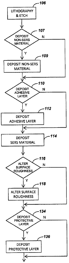
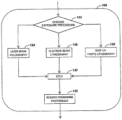
- Fabrication methods for SERS substrates in photovoltaic devices: Various fabrication methods have been developed to create effective SERS substrates for photovoltaic applications. These include lithographic techniques, chemical synthesis approaches, and self-assembly processes that can produce nanostructured surfaces with controlled morphology. Advanced deposition methods allow for precise integration of SERS substrates with photovoltaic materials. Cost-effective and scalable manufacturing processes are particularly important for commercial viability, enabling the mass production of SERS-enhanced solar cells with improved efficiency.
02 Nanoparticle-based SERS substrates for photovoltaic applications
Nanoparticle-based SERS substrates can be incorporated into photovoltaic devices to enhance their efficiency. These substrates typically consist of metal nanoparticles (such as gold, silver, or copper) that exhibit localized surface plasmon resonance, which can concentrate electromagnetic fields and increase light absorption in the active layer. By carefully controlling the size, shape, and distribution of these nanoparticles, the optical properties can be tuned to match the absorption spectrum of the photovoltaic material, leading to improved energy conversion efficiency.Expand Specific Solutions03 Characterization methods for SERS-enhanced photovoltaic materials
Various analytical techniques can be used to characterize SERS substrates and evaluate their impact on photovoltaic efficiency. These methods include Raman spectroscopy, scanning electron microscopy, atomic force microscopy, and electrical characterization techniques. By understanding the relationship between the SERS substrate structure and photovoltaic performance, researchers can optimize the design of these materials for maximum efficiency enhancement. These characterization methods help identify key parameters such as enhancement factors, hot spot distribution, and charge transfer dynamics.Expand Specific Solutions04 Fabrication techniques for SERS substrates in photovoltaic devices
Various fabrication methods can be employed to create effective SERS substrates for photovoltaic applications. These include lithographic techniques, chemical synthesis, self-assembly, template-assisted growth, and physical vapor deposition. Each method offers different advantages in terms of cost, scalability, reproducibility, and control over the nanostructure geometry. Advanced fabrication approaches enable the creation of hierarchical structures that can simultaneously enhance light trapping and charge collection, leading to significant improvements in photovoltaic efficiency.Expand Specific Solutions05 Integration of SERS substrates with different photovoltaic technologies
SERS substrates can be integrated with various photovoltaic technologies, including silicon-based solar cells, thin-film photovoltaics, organic solar cells, and perovskite solar cells. The integration strategy must be tailored to the specific photovoltaic technology to maximize efficiency enhancement while maintaining compatibility with existing manufacturing processes. Considerations include the placement of the SERS substrate (front surface, back surface, or within the active layer), the optical coupling between the substrate and the active material, and the potential impact on charge transport properties.Expand Specific Solutions
Key Industry Players in SERS-Enhanced Photovoltaic Field
The SERS substrates for photovoltaic efficiency enhancement market is currently in an early growth phase, characterized by intensive research and development activities. The market size remains relatively modest but shows promising expansion potential as photovoltaic technologies seek higher efficiency solutions. From a technical maturity perspective, the field is still evolving with academic institutions leading fundamental research while commercial applications are emerging. Key players include established technology corporations like IBM, HP, and Panasonic, alongside specialized research entities such as Fraunhofer-Gesellschaft and Shanghai Institute of Ceramics. Universities including Duke, Nanjing, and Monash are driving innovation through fundamental research, while companies like Solar Frontier and Yash Nanotech are developing commercial applications. The ecosystem demonstrates a balanced mix of academic research and industrial development, indicating a technology approaching commercial viability.
Duke University
Technical Solution: Duke University has developed innovative plasmonic nanostructures as SERS substrates for photovoltaic applications. Their approach involves the fabrication of silver and gold nanoparticle arrays with precisely controlled geometries that create localized surface plasmon resonance (LSPR) effects. These nanostructures are integrated into the photoactive layers of solar cells to enhance light absorption and charge carrier generation. The university's research demonstrates that their SERS substrates can increase the path length of incident light within the photovoltaic material by up to 40 times in specific wavelength regions. Their technology employs a cost-effective colloidal synthesis method followed by nanoimprint lithography to create large-area, uniform SERS substrates that can be incorporated into commercial photovoltaic manufacturing processes.
Strengths: Exceptional light trapping capabilities across broad spectral ranges; scalable fabrication techniques compatible with existing manufacturing processes; demonstrated enhancement of quantum efficiency in thin-film solar cells. Weaknesses: Potential long-term stability issues in outdoor conditions; optimization required for different photovoltaic material systems; higher initial production costs compared to conventional solar cell architectures.
Nanjing University
Technical Solution: Nanjing University has pioneered hierarchical SERS substrates specifically designed for photovoltaic enhancement. Their technology utilizes a dual-scale approach combining micro and nano-structured metallic surfaces to maximize electromagnetic field enhancement. The university has developed a novel sol-gel assisted nanoimprinting technique to fabricate large-area, uniform SERS substrates with controlled hot-spot density. These substrates feature silver-coated silicon nanopillars arranged in optimized patterns that generate strong plasmonic coupling effects. When integrated into perovskite solar cells, their SERS substrates have demonstrated photocurrent enhancement of up to 27% compared to reference devices. The enhanced performance is attributed to both increased light absorption and improved charge separation efficiency at the metal-semiconductor interface. Their recent work has focused on developing SERS substrates that can simultaneously enhance light harvesting and suppress carrier recombination.
Strengths: Highly reproducible fabrication process; demonstrated significant efficiency improvements in perovskite solar cells; dual functionality in enhancing both optical and electrical properties. Weaknesses: Complex manufacturing process requiring specialized equipment; potential material degradation issues at metal-semiconductor interfaces; limited testing under real-world operating conditions.
Critical Patents and Research on SERS Photovoltaic Enhancement
Surface enhanced raman spectroscopy substrates
PatentWO2010129748A2
Innovation
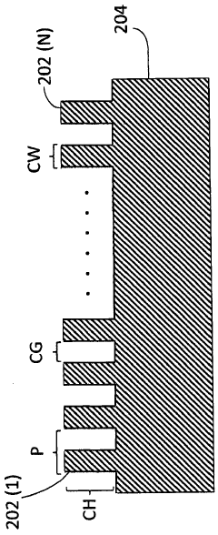
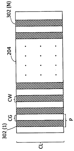
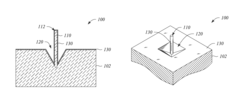
- A nanostructured substrate with multiple nanostructures, each featuring a core coated with SERS active material, where the cores are separated by core gaps and the SERS active material is separated by small SERS gaps, achieved through photolithographic techniques and etching processes, allowing for the deposition of SERS active materials like gold or silver, and optional adhesion and protective coatings to enhance performance.
Surface enhanced raman spectroscopy employing a nanorod in a surface indentation
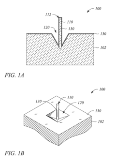
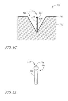
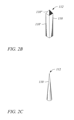
PatentInactiveUS9080980B2
Innovation
- Incorporating a nanorod into a surface indentation on a substrate, which enhances the Raman scattering signal by launching plasmons and focusing the electromagnetic field at the nanorod tip and its interface with the indentation, achieving a Raman enhancement factor exceeding 10^11.
Materials Science Considerations for SERS Substrates
The selection of materials for Surface-Enhanced Raman Spectroscopy (SERS) substrates plays a critical role in determining their effectiveness for photovoltaic applications. Noble metals, particularly gold and silver, remain the predominant materials due to their exceptional plasmonic properties in the visible to near-infrared spectrum. These metals exhibit strong localized surface plasmon resonance (LSPR), which generates intense electromagnetic fields that can significantly enhance light absorption in photovoltaic cells.
Nanostructure morphology represents another crucial consideration, with various geometries offering distinct advantages. Nanospheres provide uniform enhancement but limited hotspot density, while nanorods offer tunable resonance through aspect ratio manipulation. More complex structures such as nanostars and nanoporous architectures create numerous hotspots with field enhancement factors exceeding 10^6, potentially transforming photovoltaic efficiency parameters.
Surface roughness at the nanoscale significantly impacts SERS performance, with optimal roughness features typically ranging from 10-100 nm. This dimension allows for maximum plasmon coupling while maintaining structural stability. Recent research indicates that hierarchical roughness—combining features at multiple scale lengths—can provide broader spectral enhancement beneficial for capturing wider portions of the solar spectrum.
The substrate's stability under solar radiation presents a significant materials science challenge. Prolonged exposure to intense light and varying temperatures can lead to thermal reshaping, oxidation, and degradation of plasmonic properties. Protective coatings using ultrathin layers of alumina or silica have demonstrated effectiveness in preserving SERS activity while maintaining optical transparency essential for photovoltaic applications.
Fabrication scalability remains a critical consideration for practical implementation. While techniques like electron beam lithography produce precisely controlled nanostructures, their high cost and low throughput limit commercial viability. Chemical synthesis methods offer greater scalability but with reduced uniformity. Recent advances in nanoimprint lithography and self-assembly techniques show promise for achieving both precision and scalability.
Biocompatibility and environmental considerations have gained increasing attention, particularly for building-integrated photovoltaics. Research into alternative plasmonic materials such as aluminum, copper, and conductive nitrides aims to reduce reliance on precious metals while maintaining enhancement capabilities. These materials must balance cost-effectiveness with performance to enable widespread adoption of SERS-enhanced photovoltaic technologies.
Environmental Impact and Sustainability Assessment
The integration of Surface-Enhanced Raman Spectroscopy (SERS) substrates into photovoltaic systems presents significant environmental implications that warrant thorough assessment. The manufacturing processes for SERS substrates typically involve noble metals such as gold and silver, which require energy-intensive mining and refining operations. These processes contribute to carbon emissions and environmental degradation, potentially offsetting some of the environmental benefits gained from improved photovoltaic efficiency.
Life cycle assessment (LCA) studies indicate that the environmental footprint of SERS-enhanced photovoltaic systems depends heavily on substrate composition and fabrication methods. Conventional lithographic techniques used for creating nanostructured SERS substrates often employ hazardous chemicals and generate substantial waste. However, emerging green synthesis approaches utilizing plant extracts or microorganisms for nanoparticle production offer promising alternatives with reduced environmental impact.
The durability and longevity of SERS substrates directly influence their sustainability profile. Current research indicates that many high-performance SERS substrates suffer from degradation under prolonged exposure to environmental conditions, necessitating replacement and generating additional waste. Innovations in protective coatings and self-healing materials are being explored to extend substrate lifespan and improve overall sustainability metrics.
From a resource perspective, the reliance on scarce noble metals raises concerns about long-term sustainability. The global reserves of silver and gold are limited, and their extraction causes significant environmental disruption. Research into alternative plasmonic materials, such as aluminum, copper, and conductive polymers, represents a crucial direction for reducing dependence on rare resources while maintaining enhancement capabilities.
The end-of-life management of SERS-enhanced photovoltaic systems presents both challenges and opportunities. Recycling technologies for recovering precious metals from spent substrates are technically feasible but not yet widely implemented at commercial scale. Developing efficient recovery processes could significantly improve the circular economy profile of these technologies and mitigate resource depletion concerns.
When evaluating net environmental benefit, the increased energy conversion efficiency provided by SERS substrates must be balanced against their embodied energy and environmental costs. Preliminary studies suggest that for SERS enhancements exceeding 20% in efficiency, the environmental payback period can be reduced substantially compared to conventional photovoltaics, particularly in regions with lower solar irradiance where traditional systems struggle to achieve optimal performance.
Unlock deeper insights with Patsnap Eureka Quick Research — get a full tech report to explore trends and direct your research. Try now!
Generate Your Research Report Instantly with AI Agent
Supercharge your innovation with Patsnap Eureka AI Agent Platform!