

SERS Substrates Integration in Novel Sensor Technologies
OCT 1, 20259 MIN READ
Generate Your Research Report Instantly with AI Agent
Patsnap Eureka helps you evaluate technical feasibility & market potential.
SERS Technology Background and Objectives
Surface-Enhanced Raman Spectroscopy (SERS) emerged in the late 1970s when researchers discovered that Raman signals could be dramatically amplified when molecules were adsorbed on roughened metal surfaces. This phenomenon, initially observed on electrochemically roughened silver electrodes, demonstrated enhancement factors of 105-106, revolutionizing the field of molecular detection. Over the past four decades, SERS technology has evolved from a laboratory curiosity to a powerful analytical tool with diverse applications across multiple industries.
The technological evolution of SERS has been marked by significant breakthroughs in substrate design, moving from simple roughened surfaces to sophisticated nanostructured materials. Early developments focused on colloidal metal nanoparticles, while recent advances have introduced precisely engineered substrates with controlled hot spots, enabling reproducible signal enhancement. This progression has been driven by parallel advancements in nanofabrication techniques, computational modeling, and fundamental understanding of plasmonic phenomena.
Current SERS technology trends indicate a shift toward integrated sensing platforms that combine SERS substrates with microfluidics, portable spectrometers, and automated data analysis systems. The miniaturization of SERS-based devices and their integration with other sensing modalities represent key directions in the field's development. Additionally, there is growing interest in flexible and conformable SERS substrates that can adapt to various sample geometries and in-situ monitoring applications.
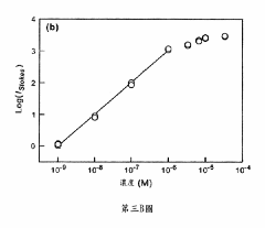
The primary objective of SERS substrate integration in novel sensor technologies is to develop highly sensitive, selective, and reliable detection platforms for real-time analysis in complex environments. Specific technical goals include achieving consistent enhancement factors exceeding 108, developing manufacturing processes for cost-effective mass production of SERS substrates, and creating standardized protocols for substrate characterization and performance evaluation.
Another critical objective is to bridge the gap between laboratory demonstrations and practical field applications by addressing challenges related to substrate stability, shelf-life, and performance in diverse environmental conditions. The integration of SERS substrates with emerging technologies such as artificial intelligence for spectral analysis, Internet of Things (IoT) connectivity for remote monitoring, and smartphone-based detection platforms represents a frontier with immense potential for democratizing advanced analytical capabilities.
The ultimate aim is to position SERS-based sensing as a versatile analytical tool capable of addressing pressing challenges in healthcare diagnostics, environmental monitoring, food safety, and security applications, thereby transforming how we detect and analyze molecular species across multiple industries and scientific disciplines.
The technological evolution of SERS has been marked by significant breakthroughs in substrate design, moving from simple roughened surfaces to sophisticated nanostructured materials. Early developments focused on colloidal metal nanoparticles, while recent advances have introduced precisely engineered substrates with controlled hot spots, enabling reproducible signal enhancement. This progression has been driven by parallel advancements in nanofabrication techniques, computational modeling, and fundamental understanding of plasmonic phenomena.
Current SERS technology trends indicate a shift toward integrated sensing platforms that combine SERS substrates with microfluidics, portable spectrometers, and automated data analysis systems. The miniaturization of SERS-based devices and their integration with other sensing modalities represent key directions in the field's development. Additionally, there is growing interest in flexible and conformable SERS substrates that can adapt to various sample geometries and in-situ monitoring applications.
The primary objective of SERS substrate integration in novel sensor technologies is to develop highly sensitive, selective, and reliable detection platforms for real-time analysis in complex environments. Specific technical goals include achieving consistent enhancement factors exceeding 108, developing manufacturing processes for cost-effective mass production of SERS substrates, and creating standardized protocols for substrate characterization and performance evaluation.
Another critical objective is to bridge the gap between laboratory demonstrations and practical field applications by addressing challenges related to substrate stability, shelf-life, and performance in diverse environmental conditions. The integration of SERS substrates with emerging technologies such as artificial intelligence for spectral analysis, Internet of Things (IoT) connectivity for remote monitoring, and smartphone-based detection platforms represents a frontier with immense potential for democratizing advanced analytical capabilities.
The ultimate aim is to position SERS-based sensing as a versatile analytical tool capable of addressing pressing challenges in healthcare diagnostics, environmental monitoring, food safety, and security applications, thereby transforming how we detect and analyze molecular species across multiple industries and scientific disciplines.
Market Analysis for SERS-Based Sensing Solutions
The global market for Surface-Enhanced Raman Spectroscopy (SERS)-based sensing solutions has experienced remarkable growth in recent years, driven by increasing demand for highly sensitive detection methods across multiple industries. The market size was valued at approximately $1.2 billion in 2022 and is projected to reach $2.8 billion by 2028, representing a compound annual growth rate (CAGR) of 15.2% during the forecast period.
Healthcare and life sciences currently dominate the SERS sensor market, accounting for nearly 45% of the total market share. This sector's prominence stems from the growing need for rapid, accurate diagnostic tools and point-of-care testing solutions. The pharmaceutical industry has also embraced SERS technology for drug discovery and quality control processes, contributing significantly to market expansion.
Environmental monitoring represents another rapidly growing application segment, with a projected CAGR of 18.7% through 2028. Government regulations mandating stricter pollution control and water quality monitoring have accelerated adoption in this sector. Food safety testing applications are similarly gaining traction, particularly in developed economies with stringent food quality standards.
Regionally, North America leads the market with approximately 38% share, followed by Europe (29%) and Asia-Pacific (24%). However, the Asia-Pacific region is expected to witness the fastest growth rate due to increasing R&D investments, expanding healthcare infrastructure, and rising environmental concerns in countries like China, Japan, and South Korea.
Key market drivers include technological advancements in SERS substrate fabrication, miniaturization of sensing devices, and integration with portable/handheld instruments. The growing trend toward point-of-need testing across various applications has created significant opportunities for SERS-based solutions that offer rapid results without requiring sophisticated laboratory infrastructure.
Market challenges include high initial costs associated with SERS equipment, technical complexity requiring specialized expertise, and competition from alternative sensing technologies. Additionally, standardization issues and reproducibility concerns have somewhat limited widespread adoption in certain applications.
The competitive landscape features both established analytical instrument manufacturers and innovative startups. Major players include Thermo Fisher Scientific, Horiba, Bruker, Ocean Insight, and Renishaw, collectively holding approximately 65% market share. Meanwhile, emerging companies like Metrohm Raman, Real-Time Analyzers, and Enhanced Spectrometry are gaining ground through specialized SERS substrate innovations and application-specific solutions.
Current SERS Substrate Challenges and Limitations
Despite significant advancements in SERS substrate technology, several critical challenges continue to impede the seamless integration of these substrates into novel sensor technologies. One of the primary limitations is reproducibility, as current manufacturing processes often yield substrates with inconsistent enhancement factors across different batches. This variability significantly impacts the reliability of quantitative measurements, making standardization difficult for commercial applications.
Stability presents another major challenge, with many high-performance SERS substrates exhibiting degradation over time or under varying environmental conditions. This instability manifests as signal drift, reduced enhancement capability, or complete substrate failure, particularly problematic for long-term monitoring applications or field deployments where controlled conditions cannot be maintained.
Cost-effectiveness remains a substantial barrier to widespread adoption. Current high-performance SERS substrates often require expensive nanofabrication techniques such as electron beam lithography or complex chemical synthesis processes. These manufacturing constraints limit scalability and increase per-unit costs, restricting their application primarily to research settings rather than commercial sensor platforms.
Integration complexity poses significant engineering challenges when incorporating SERS substrates into functional sensor devices. The interface between the substrate and other sensor components (microfluidics, electronics, optical systems) often requires specialized solutions that are difficult to standardize across different sensing platforms. This complexity extends development timelines and increases failure rates during prototype stages.
Sensitivity to sample preparation represents another critical limitation. Many current SERS substrates perform optimally only under specific sample conditions, requiring extensive pre-processing steps that complicate real-world applications. This dependency on precise sample preparation protocols limits the applicability of SERS-based sensors in point-of-care or field settings where simplified workflows are essential.
Selectivity issues persist across various substrate types, with many exhibiting non-specific binding that produces confounding signals in complex sample matrices. This lack of molecular specificity necessitates additional separation steps or complex data processing algorithms to extract meaningful information from the enhanced spectra.
Miniaturization challenges further complicate integration efforts, as maintaining enhancement performance while reducing substrate dimensions remains technically difficult. This limitation particularly affects the development of portable or wearable SERS-based sensing technologies where space constraints are significant design factors.
Current SERS Substrate Integration Approaches
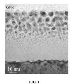
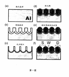
01 Metallic nanostructured SERS substrates
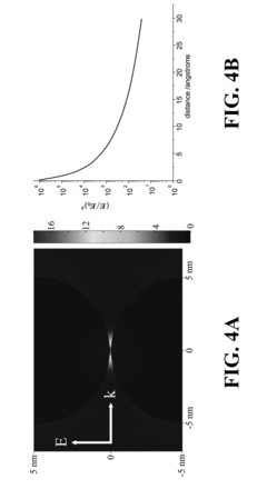
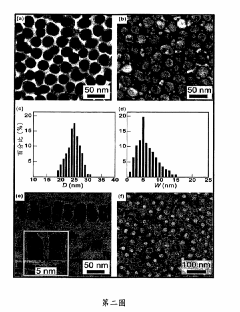
Metallic nanostructured surfaces are widely used as SERS substrates due to their ability to enhance Raman signals through plasmonic effects. These substrates typically consist of noble metals like gold, silver, or copper arranged in specific patterns or structures such as nanoparticles, nanorods, or nanogaps. The size, shape, and spacing of these metallic nanostructures can be optimized to achieve maximum enhancement factors, enabling sensitive detection of analytes at low concentrations.- Metallic nanostructured SERS substrates: Metallic nanostructured surfaces are widely used as SERS substrates due to their ability to enhance Raman signals through localized surface plasmon resonance. These substrates typically consist of noble metals like gold, silver, or copper arranged in specific patterns or geometries such as nanoparticles, nanorods, or nanogaps. The size, shape, and spacing of these metallic nanostructures can be optimized to achieve maximum enhancement factors for sensitive molecular detection.
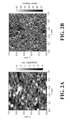
- Fabrication methods for SERS substrates: Various fabrication techniques are employed to create effective SERS substrates, including lithography, chemical deposition, self-assembly, and template-assisted methods. Advanced manufacturing approaches like nanoimprint lithography, electron beam lithography, and colloidal assembly enable precise control over the substrate architecture. These methods allow for reproducible production of substrates with consistent enhancement factors, which is crucial for quantitative SERS applications in analytical chemistry and biosensing.
- Flexible and portable SERS substrates: Flexible SERS substrates are designed for field applications and point-of-care diagnostics. These substrates are typically fabricated on polymer or paper-based materials that can conform to various surfaces while maintaining their enhancement capabilities. The flexibility allows for direct sampling from curved surfaces and integration into wearable sensors. Portable SERS platforms combine these flexible substrates with miniaturized detection systems for on-site chemical and biological analysis.
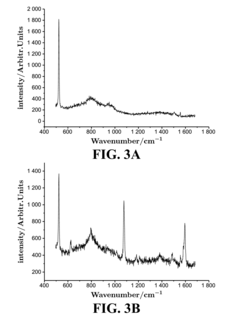
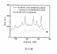
- SERS substrate applications in biosensing and medical diagnostics: SERS substrates are increasingly used for biosensing and medical diagnostic applications due to their high sensitivity and specificity. These substrates can be functionalized with recognition elements like antibodies, aptamers, or molecularly imprinted polymers to selectively capture target biomarkers. The enhanced Raman signals allow for detection of disease markers, pathogens, and toxins at ultralow concentrations, making them valuable tools for early disease detection, food safety testing, and environmental monitoring.
- Novel materials and hybrid SERS substrates: Research is focused on developing novel materials and hybrid structures to improve SERS performance. These include semiconductor-metal composites, graphene-enhanced substrates, and metal-organic frameworks. Hybrid SERS substrates often combine plasmonic materials with other functional components to achieve multifunctionality, such as simultaneous detection and separation capabilities. These advanced materials can provide higher enhancement factors, better stability, and additional functionalities compared to traditional metallic SERS substrates.
02 Fabrication methods for SERS substrates
Various fabrication techniques are employed to create effective SERS substrates with controlled morphology and reproducible enhancement factors. These methods include lithographic techniques, chemical synthesis, template-assisted growth, and self-assembly processes. Advanced manufacturing approaches such as nanoimprint lithography, electron beam lithography, and colloidal assembly enable precise control over the substrate architecture, which is crucial for achieving consistent SERS performance across different batches and applications.Expand Specific Solutions03 Flexible and portable SERS substrates
Flexible and portable SERS substrates have been developed to enable on-site detection and analysis in various environments. These substrates are typically fabricated on flexible polymeric materials or paper-based platforms that can conform to irregular surfaces while maintaining their enhancement capabilities. The portability aspect allows for field-deployable SERS sensing without the need for complex laboratory equipment, making them suitable for environmental monitoring, food safety testing, and point-of-care diagnostics.Expand Specific Solutions04 SERS substrate integration with microfluidics
Integration of SERS substrates with microfluidic systems enables automated sample handling, concentration, and analysis. These integrated platforms combine the sensitivity of SERS detection with the precise fluid control capabilities of microfluidics, allowing for efficient sample preparation and reduced analysis time. Microfluidic SERS devices can incorporate multiple functions such as mixing, separation, and detection on a single chip, making them valuable tools for high-throughput screening and multiplexed sensing applications.Expand Specific Solutions05 SERS substrate applications in biosensing and chemical detection
SERS substrates are extensively used for biosensing and chemical detection applications due to their ability to provide molecular fingerprint information with high sensitivity. These substrates can be functionalized with specific recognition elements such as antibodies, aptamers, or molecularly imprinted polymers to enhance selectivity toward target analytes. Applications include detection of pathogens, biomarkers, environmental pollutants, explosives, and pharmaceutical compounds, with detection limits often reaching single-molecule levels under optimized conditions.Expand Specific Solutions
Leading Companies and Research Institutions in SERS Technology
SERS Substrates Integration in Novel Sensor Technologies is currently in an early growth phase, characterized by rapid technological advancement but limited commercial maturity. The market is expanding steadily, projected to reach significant value as applications in healthcare, environmental monitoring, and security gain traction. From a technological standpoint, companies like HP Development Co. LP and Seiko Epson Corp. are leveraging their expertise in precision manufacturing to develop commercial SERS platforms, while research institutions such as Agency for Science, Technology & Research and Korea Advanced Institute of Science & Technology are driving fundamental innovations. Baxter International and SICPA Holding SA are exploring specialized applications in healthcare diagnostics and security authentication respectively, indicating the technology's cross-industry potential.
Agency for Science, Technology & Research
Technical Solution: The Agency for Science, Technology & Research (A*STAR) has developed advanced SERS substrates using nanofabrication techniques that combine gold nanoparticles with specialized polymer matrices. Their approach focuses on creating highly uniform and reproducible SERS substrates through controlled self-assembly processes. A*STAR's technology incorporates precise nanogap engineering to create consistent "hot spots" that enhance Raman signals by factors exceeding 10^8. Their substrates feature specialized surface chemistry modifications that enable selective binding to target analytes, making them particularly effective for environmental monitoring and food safety applications. A*STAR has also pioneered integration methods for incorporating these SERS substrates directly into microfluidic platforms, creating complete lab-on-chip sensing solutions that require minimal sample preparation.
Strengths: Exceptional reproducibility and uniformity of enhancement factors across substrates; excellent integration capabilities with existing microfluidic technologies; strong performance in aqueous environments. Weaknesses: Higher production costs compared to simpler SERS substrates; requires specialized equipment for fabrication; limited shelf-life without proper storage conditions.
IMRA America, Inc.
Technical Solution: IMRA America has developed proprietary SERS substrate technology utilizing femtosecond laser processing to create precisely controlled nanostructured surfaces. Their approach employs ultrafast laser ablation to generate self-organized nanostructures on metal surfaces, creating reproducible SERS-active sites. The company's technology enables direct writing of SERS-active patterns onto various sensor platforms, facilitating seamless integration. IMRA's substrates feature specialized surface treatments that enhance durability and stability in harsh environments, making them suitable for industrial applications. Their manufacturing process allows for scalable production of SERS substrates with consistent enhancement factors across large areas, addressing a key challenge in commercialization. IMRA has also developed proprietary packaging solutions that maintain substrate performance during storage and transportation.
Strengths: Direct integration capability with existing sensor platforms; excellent durability in harsh environmental conditions; scalable manufacturing process. Weaknesses: Higher initial equipment investment for femtosecond laser systems; limited flexibility in substrate material selection; requires precise control of laser parameters.
Key Patents and Breakthroughs in SERS Substrate Design
Substrates for surface enhanced raman spectroscopy
PatentInactiveUS20160274031A1
Innovation
- A method involving high dose metal ion implantation into substrates to form metal nano-particle/substrate composites, where the substrate is ion implanted with metal ions to exceed solid solubility limits, followed by thermal annealing and selective etching to expose nano-particles, allowing for controlled particle size and separation, and enabling the use of various substrate materials and geometries.
Substrate for surface-enhanced raman spectroscopy, SERS sensors, and method for preparing same
PatentActiveTW200801486A
Innovation
- A method involving the fabrication of a template with cavities, etching to enlarge and separate them by 3 to 50 nm, placing metal particles, and further etching to expose them, using anodized aluminum oxide templates and electrochemical plating to create uniform nanoparticle arrays.
Manufacturing Scalability of SERS Substrates
The scalability of SERS substrate manufacturing represents a critical bottleneck in the widespread adoption of SERS-based sensor technologies. Current laboratory-scale production methods, while effective for research purposes, face significant challenges when transitioning to industrial-scale manufacturing. Traditional fabrication techniques such as electron beam lithography and focused ion beam milling offer precise control over nanostructure geometry but remain prohibitively expensive and time-consuming for mass production scenarios.
Recent advances in nanofabrication have introduced more scalable approaches, including nanoimprint lithography, template-assisted electrochemical deposition, and self-assembly techniques. Nanoimprint lithography, in particular, has demonstrated promising results for high-throughput SERS substrate production, achieving feature sizes below 20 nm while maintaining consistency across large surface areas. This technique reduces the cost per unit by approximately 60-70% compared to conventional lithography methods when implemented at scale.
Roll-to-roll manufacturing processes represent another significant advancement, enabling continuous production of flexible SERS substrates on polymer films. This approach has achieved production speeds of up to 10 meters per minute while maintaining enhancement factor uniformity within ±15% across the substrate. Such techniques are particularly valuable for integrating SERS substrates into wearable and point-of-care diagnostic devices where flexibility and low cost are paramount.
Quality control remains a significant challenge in scaled manufacturing environments. Variations in nanostructure dimensions as small as 5-10 nm can dramatically impact SERS enhancement factors, necessitating robust in-line monitoring systems. Advanced optical characterization techniques, including automated Raman mapping and hyperspectral imaging, are being integrated into production lines to ensure batch-to-batch consistency and performance reliability.
Cost considerations also play a crucial role in manufacturing scalability. Current production costs for high-performance SERS substrates range from $5-20 per cm², significantly limiting their application in disposable sensing devices. Material innovations, including the replacement of noble metals with plasmonic alloys or core-shell nanostructures, have shown potential to reduce material costs by 30-40% while maintaining comparable enhancement factors.
Environmental sustainability presents an emerging concern in scaled manufacturing operations. Traditional SERS substrate fabrication often involves hazardous chemicals and significant energy consumption. Green chemistry approaches, including aqueous-based synthesis methods and biodegradable template materials, are being developed to reduce environmental impact while maintaining performance metrics. These sustainable manufacturing protocols will be essential for meeting increasingly stringent environmental regulations as production volumes increase.
Environmental and Biocompatibility Considerations
The integration of SERS substrates into novel sensor technologies necessitates careful consideration of environmental impacts and biocompatibility factors. Current SERS substrate materials, including noble metals like gold and silver, pose potential environmental concerns related to resource depletion and waste generation during manufacturing processes. The extraction and processing of these metals involve energy-intensive operations that contribute to carbon emissions and ecological disruption. Additionally, the disposal of used SERS-based sensors may lead to environmental contamination if not properly managed, particularly when nanoparticles enter aquatic ecosystems.
Biocompatibility represents a critical consideration for SERS substrates in biological sensing applications. Direct contact between metallic nanostructures and biological systems may trigger immune responses, inflammation, or cytotoxicity. Recent studies have documented varying degrees of cellular toxicity associated with different SERS substrate materials, with factors such as particle size, surface chemistry, and concentration significantly influencing biological interactions. Silver nanoparticles, while offering excellent SERS enhancement, generally exhibit higher cytotoxicity compared to gold counterparts, limiting their application in in vivo sensing.
Surface functionalization strategies have emerged as effective approaches to mitigate biocompatibility concerns. The application of biocompatible coatings, such as polyethylene glycol (PEG), phospholipids, or specific proteins, can create a protective barrier between the metallic substrate and biological components. These modifications not only reduce potential toxicity but also enhance the specificity and stability of SERS sensors in complex biological environments. Furthermore, biodegradable SERS substrates represent a promising direction, allowing for temporary diagnostic applications without long-term biological accumulation.
Regulatory frameworks governing the environmental and health impacts of nanomaterials continue to evolve globally. The European Union's REACH regulation and the FDA's guidelines for nanomaterials in medical devices establish important benchmarks for safety assessment. Compliance with these regulations requires comprehensive toxicological profiling and environmental impact assessments throughout the product lifecycle. Manufacturers developing SERS-based sensing technologies must navigate these regulatory landscapes while demonstrating both efficacy and safety.
Sustainable design principles are increasingly being incorporated into next-generation SERS substrate development. Green synthesis methods utilizing plant extracts or microorganisms for nanoparticle production offer reduced environmental footprints compared to conventional chemical reduction approaches. Additionally, the exploration of alternative, more abundant materials such as copper, aluminum, or carbon-based structures may address resource scarcity concerns while maintaining acceptable sensing performance. Life cycle assessment methodologies are becoming essential tools for evaluating the holistic environmental impact of SERS-based sensing technologies from production through disposal.
Unlock deeper insights with Patsnap Eureka Quick Research — get a full tech report to explore trends and direct your research. Try now!
Generate Your Research Report Instantly with AI Agent
Supercharge your innovation with Patsnap Eureka AI Agent Platform!