Spin Qubits in Silicon: Integration with Quantum Sensors
OCT 10, 20259 MIN READ
Generate Your Research Report Instantly with AI Agent
Patsnap Eureka helps you evaluate technical feasibility & market potential.
Silicon Spin Qubit Background and Objectives
Silicon spin qubits have emerged as a promising platform for quantum computing due to their compatibility with existing semiconductor manufacturing technologies. The evolution of this technology can be traced back to the early 2000s when researchers first demonstrated the ability to isolate and manipulate single electron spins in silicon quantum dots. Since then, significant advancements have been made in improving coherence times, gate fidelities, and scalability of silicon-based quantum systems.
The technological trajectory of silicon spin qubits has been characterized by steady improvements in material purity, fabrication techniques, and control electronics. Early challenges included the presence of nuclear spins in natural silicon that limited coherence times. This led to the development of isotopically purified silicon-28, which dramatically extended qubit lifetimes by removing the magnetic noise from nuclear spins.
Current research is focused on integrating silicon spin qubits with quantum sensors to enhance measurement precision and enable new applications. Quantum sensors, which leverage quantum mechanical properties to achieve unprecedented sensitivity, can significantly improve the readout fidelity and initialization of spin qubits. This integration represents a convergence of two powerful quantum technologies with potential synergistic benefits.
The primary technical objectives in this field include achieving high-fidelity qubit operations with error rates below the threshold for quantum error correction, developing scalable architectures capable of supporting thousands of qubits, and creating robust interfaces between spin qubits and quantum sensing elements. Additionally, researchers aim to demonstrate practical quantum advantage in specific applications such as quantum simulation of materials and optimization problems.
Long-term goals involve the development of fault-tolerant quantum computers based on silicon spin qubits integrated with advanced quantum sensing capabilities. This would enable applications in cryptography, drug discovery, materials science, and financial modeling that are currently intractable for classical computers.
The integration of quantum sensors with silicon spin qubits also opens new possibilities for quantum metrology and sensing applications. These include magnetic field sensing with unprecedented sensitivity, detection of single molecules for medical diagnostics, and gravitational field mapping for geological exploration.
As the field progresses, we anticipate a convergence of quantum computing and quantum sensing technologies, leading to hybrid systems that leverage the strengths of both domains. This convergence represents a significant opportunity for technological innovation and scientific discovery in the coming decades.
Market Analysis for Quantum Computing Applications
The quantum computing market is experiencing unprecedented growth, with projections indicating a market value reaching $1.7 billion by 2026 and potentially $65 billion by 2030. Silicon-based spin qubits represent a particularly promising segment within this expanding market due to their compatibility with existing semiconductor manufacturing infrastructure, potentially lowering barriers to commercial scalability.
Current market analysis reveals that quantum computing applications are diversifying across multiple sectors. Financial services lead adoption with approximately 30% of quantum computing investments directed toward portfolio optimization, risk assessment, and fraud detection algorithms. The pharmaceutical industry follows closely, allocating significant resources to quantum-enhanced drug discovery processes that could potentially reduce development timelines by 40-60%.
Silicon spin qubits integrated with quantum sensors are positioned to capture substantial market share in precision measurement applications. The quantum sensing market itself is projected to grow at a CAGR of 15.2% through 2028, creating synergistic opportunities for integrated spin qubit technologies. Industries requiring ultra-precise measurements, including healthcare diagnostics, geological surveying, and autonomous navigation systems, represent high-value target markets.
Market segmentation analysis indicates that early commercial applications for silicon spin qubits with integrated quantum sensors will likely emerge in three primary areas: medical imaging enhancement, materials science research, and advanced navigation systems. The medical imaging segment alone represents a $2.1 billion opportunity by 2025 for quantum-enhanced technologies.
Geographical market distribution shows North America currently leading in quantum computing investments (42%), followed by Europe (28%) and Asia-Pacific (24%). However, China's national quantum initiative is accelerating regional growth in Asia, with annual investments exceeding $10 billion. This shifting landscape suggests emerging market opportunities for silicon-based quantum technologies across diverse global regions.
Customer adoption analysis reveals that enterprise-level organizations with significant R&D budgets currently dominate the quantum computing customer base. However, the integration of spin qubits with quantum sensors could potentially expand market accessibility to mid-sized organizations through more specialized, application-specific quantum solutions.
Market barriers include the high technical expertise required for implementation, regulatory uncertainties regarding quantum technologies, and competition from alternative quantum computing architectures. Nevertheless, silicon spin qubits maintain competitive advantages in scalability, operating temperature requirements, and manufacturing compatibility that position them favorably for commercial applications requiring both quantum computation and sensing capabilities.
The market timing analysis suggests that silicon spin qubit technologies integrated with quantum sensors will reach commercial viability for specialized applications within 3-5 years, with broader market penetration expected in the 5-8 year timeframe as technical challenges around coherence times and error rates are addressed.
Current Challenges in Silicon Spin Qubit Technology
Despite significant advancements in silicon spin qubit technology, several critical challenges continue to impede the full realization of practical quantum computing systems based on this platform. The primary obstacle remains coherence time limitations, with typical T2 times for silicon spin qubits ranging from microseconds to milliseconds—still insufficient for complex quantum algorithms requiring millions of operations. Environmental noise sources, particularly from nuclear spins, charge fluctuations, and phonon interactions, contribute significantly to decoherence despite silicon's inherently low nuclear spin content.
Qubit control and readout fidelity present another substantial hurdle. Current single-qubit gate fidelities hover around 99.9%, while two-qubit gates typically achieve only 98-99% fidelity—well below the threshold required for fault-tolerant quantum computing. The integration of high-precision control electronics with quantum processors operating at millikelvin temperatures creates significant engineering challenges, particularly regarding heat dissipation and signal integrity.
Scalability remains perhaps the most formidable challenge. While laboratory demonstrations have shown promising results with small arrays of qubits, scaling to hundreds or thousands of qubits introduces complications in wiring, crosstalk, and uniform qubit performance. The fabrication process variability leads to significant qubit-to-qubit parameter variations, requiring individual calibration procedures that become exponentially complex as system size increases.
The integration of quantum sensors with silicon spin qubits introduces additional technical difficulties. Maintaining sensor sensitivity while preserving qubit coherence requires careful engineering of the interface between these systems. Sensors often introduce additional noise sources that can degrade qubit performance, creating a fundamental tension between measurement precision and qubit quality.
Material interface issues further complicate development efforts. The silicon-oxide interface, critical for defining quantum dots, exhibits charge traps and defects that contribute to decoherence. Advanced materials engineering approaches, including isotopically purified silicon-28 substrates, have shown improvements but remain challenging to implement at scale with high yield.
Power management and thermal control represent significant engineering challenges, particularly as systems scale. Cryogenic cooling capacity limits the number of control lines and active components that can operate simultaneously, creating a bottleneck for large-scale implementations. Additionally, the development of cryogenic control electronics remains in its infancy, with few commercially viable solutions available.
Addressing these challenges requires interdisciplinary collaboration spanning quantum physics, materials science, electrical engineering, and computer science. Recent research directions focus on error-resilient qubit designs, improved materials interfaces, and novel control schemes that may eventually overcome these limitations.
Existing Integration Solutions for Spin Qubits and Sensors
01 Silicon-based quantum dot spin qubits
Silicon quantum dots can be used to create spin qubits for quantum computing applications. These structures confine electrons in silicon, allowing their spin states to be manipulated and measured. Silicon quantum dots offer advantages such as long coherence times and compatibility with existing semiconductor manufacturing processes, making them promising candidates for scalable quantum computing architectures.- Silicon-based quantum dot spin qubits: Silicon quantum dots can be engineered to trap and manipulate electron spins as qubits. These structures provide excellent coherence properties due to the low nuclear spin content of silicon, especially isotopically purified silicon-28. The quantum dots can be formed using various semiconductor fabrication techniques, allowing for precise control of electron confinement and spin states, which is essential for quantum computing applications.
- Multi-qubit architectures and coupling mechanisms: Advanced architectures for silicon spin qubits involve multiple qubits arranged in arrays or networks with various coupling mechanisms. These designs enable two-qubit gates and entanglement operations necessary for quantum computing. Coupling between qubits can be achieved through exchange interactions, cavity-mediated coupling, or shuttle-based approaches, allowing for scalable quantum processor designs while maintaining the high coherence properties of silicon spin qubits.
- Control and readout techniques for silicon spin qubits: Various methods have been developed for controlling and reading out the state of spin qubits in silicon. These include electrical control using microwave pulses, magnetic field manipulation, and gate voltage modulation. Readout techniques often employ spin-to-charge conversion, radio frequency reflectometry, or dispersive readout methods. These approaches enable high-fidelity qubit operations while minimizing decoherence effects in silicon-based quantum computing systems.
- Integration with classical electronics and scalability: Silicon spin qubits offer significant advantages for integration with conventional CMOS electronics and scaling to large numbers of qubits. Fabrication techniques compatible with semiconductor manufacturing processes enable the creation of dense qubit arrays with integrated control and readout circuitry. This compatibility with existing silicon technology provides a pathway toward practical quantum processors with thousands or millions of qubits operating at low temperatures.
- Error correction and quantum algorithms for silicon spin systems: Implementing quantum error correction codes and algorithms on silicon spin qubit platforms is essential for fault-tolerant quantum computing. Various approaches have been developed to mitigate errors arising from decoherence, control imperfections, and environmental noise. These include surface codes, dynamical decoupling sequences, and hardware-efficient quantum algorithms specifically designed for the constraints and advantages of silicon spin qubit systems.
02 Fabrication methods for silicon spin qubits
Various fabrication techniques are employed to create spin qubits in silicon. These methods include lithographic patterning of silicon substrates, ion implantation for creating quantum dots, and deposition of gate electrodes for controlling electron confinement and manipulation. Advanced fabrication processes enable precise control over qubit parameters and improve reproducibility, which is essential for scaling up quantum computing systems.Expand Specific Solutions03 Control and readout mechanisms for silicon spin qubits
Effective control and readout of spin qubits in silicon requires specialized mechanisms. These include electrical gate structures for manipulating electron spins, microwave resonators for qubit control, and sensitive charge sensors for spin state detection. Advanced readout techniques enable high-fidelity measurement of qubit states, which is crucial for quantum error correction and reliable quantum computation.Expand Specific Solutions04 Quantum computing architectures using silicon spin qubits
Silicon spin qubits can be integrated into various quantum computing architectures. These architectures include linear arrays of qubits, two-dimensional lattices, and modular designs with interconnects between qubit clusters. The architectures address challenges such as qubit connectivity, control line routing, and scalability, which are essential for building practical quantum computers capable of solving complex problems.Expand Specific Solutions05 Error correction and noise mitigation in silicon spin qubits
Maintaining qubit coherence and mitigating errors is crucial for silicon spin qubit systems. Techniques include dynamical decoupling sequences to extend coherence times, materials engineering to reduce noise sources, and implementation of quantum error correction codes. Advanced error mitigation strategies enable more reliable quantum operations, which is necessary for achieving fault-tolerant quantum computation with silicon spin qubits.Expand Specific Solutions
Leading Organizations in Quantum Integration Research
Spin qubits in silicon technology is currently in an early development phase, with a growing market expected to reach significant scale as quantum computing matures. The competitive landscape features established research institutions (MIT, Delft University of Technology) collaborating with emerging specialized companies like Silicon Quantum Computing and C12 Quantum Electronics. Major semiconductor players including Intel and GlobalFoundries are investing in silicon-based quantum technologies, while national laboratories (CEA, AIST) provide critical research infrastructure. The technology is approaching the transition from fundamental research to early commercialization, with companies like Origin Quantum developing supporting software ecosystems. Integration with quantum sensors represents a key technical challenge that could accelerate practical applications.
Delft University of Technology
Technical Solution: Delft University of Technology has developed a sophisticated platform for silicon spin qubits integrated with quantum sensors. Their approach utilizes CMOS-compatible fabrication techniques to create quantum dots in silicon that trap individual electrons, whose spins serve as qubits. A distinctive feature of Delft's technology is the integration of nanoscale superconducting quantum interference devices (nanoSQUIDs) as highly sensitive magnetometers capable of detecting the magnetic moment of a single electron spin. These integrated sensors achieve measurement sensitivities approaching the quantum limit. Delft researchers have also pioneered the use of cryo-CMOS electronics co-integrated with silicon spin qubits, enabling on-chip control and readout electronics that operate at millikelvin temperatures. This integration significantly reduces the wiring complexity that typically limits quantum processor scalability. Their recent breakthroughs include demonstrating entanglement between spin qubits in silicon with high fidelity (>99%) and developing a four-qubit quantum processor with integrated control electronics, representing a significant step toward scalable quantum computing architectures.
Strengths: CMOS-compatible fabrication enabling integration with classical electronics; high-sensitivity quantum sensors approaching fundamental limits; advanced cryo-electronics integration reducing system complexity. Weaknesses: Challenges in maintaining coherence with integrated electronics nearby; thermal management issues at millikelvin temperatures; limited qubit connectivity constraining algorithm implementation.
Silicon Quantum Computing Pty Ltd.
Technical Solution: Silicon Quantum Computing (SQC) has developed a comprehensive approach to silicon spin qubits integrated with quantum sensors. Their technology is based on phosphorus donor atoms precisely positioned in a silicon lattice using scanning tunneling microscope (STM) lithography. This atomic-scale fabrication enables the creation of qubits with exceptionally long coherence times (>30 seconds in isotopically purified silicon). SQC's integration of quantum sensors involves on-chip single-electron transistors (SETs) that function as highly sensitive electrometers to detect the charge state of individual qubits. These SETs provide real-time readout capabilities with minimal disturbance to the quantum system. Additionally, SQC has demonstrated the ability to couple multiple qubits through exchange interactions while maintaining quantum coherence, a critical step toward scalable quantum computing architectures. Their recent advancements include the development of a two-qubit logic gate in silicon with fidelities approaching 99%, demonstrating the potential for fault-tolerant quantum computation.
Strengths: Exceptional qubit coherence times in silicon; atomic-precision fabrication enabling reproducible qubit properties; compatibility with existing semiconductor manufacturing infrastructure. Weaknesses: Challenges in scaling to large numbers of qubits; sensitivity to environmental noise requiring extensive error correction; relatively slow gate operations compared to some competing technologies.
Key Patents in Silicon Spin Qubit-Sensor Integration
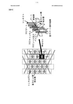
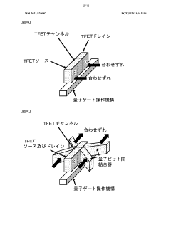
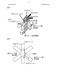
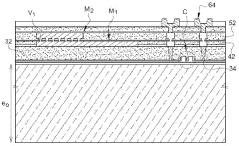
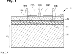
Silicon spin quantum bit device and manufacturing method therefor
PatentWO2021229987A1
Innovation
- A manufacturing method involving the formation of a dummy gate for self-alignment of the tunnel field effect transistor, quantum gate, and inter-qubit coupler, with the channel region formed in a silicon film, allowing for improved alignment and reduced variations, and the use of self-aligned processes to embed the quantum gate and inter-qubit coupler, enhancing the qubit's integration and coherence.
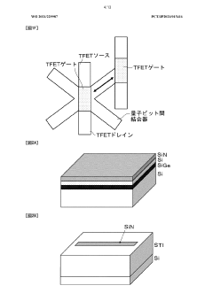
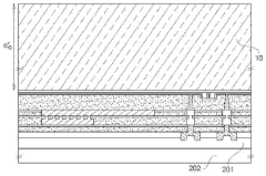
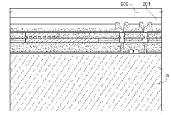
BACK GRID FOR QUANTUM DEVICE
PatentActiveFR3131086A1
Innovation
- A quantum device with a rear electrostatic control grid formed by a conductive layer lining the side walls and bottom of an opening in a semiconductor support layer, extending to an insulating layer, which maintains mechanical strength and reduces stress, using a semiconductor-on-insulator substrate with a conductive layer deposited through the opening.
Quantum Error Correction Strategies
Quantum Error Correction (QEC) represents a critical frontier for advancing spin qubits in silicon, particularly when integrated with quantum sensors. The fundamental challenge stems from quantum systems' inherent vulnerability to decoherence and operational errors. For silicon-based spin qubits, these errors manifest primarily through magnetic field fluctuations, charge noise, and hyperfine interactions with nuclear spins. Conventional QEC codes like the surface code require significant qubit overhead, presenting implementation challenges for current silicon quantum processors.
Recent advancements have focused on tailoring QEC strategies specifically for silicon spin qubits. The development of dynamical decoupling sequences optimized for the silicon environment has shown promising results in extending coherence times. These sequences effectively filter out environmental noise at specific frequencies, creating protected operational windows for quantum information processing while maintaining compatibility with quantum sensing operations.
Hardware-efficient QEC codes represent another significant development path. These codes leverage the natural properties of silicon spin systems to reduce the overhead required for error correction. Notably, the use of bosonic codes adapted for spin ensembles in silicon has demonstrated error suppression capabilities while maintaining the quantum sensing functionality essential for integrated applications.
Autonomous error correction protocols have emerged as particularly valuable for silicon spin qubit-sensor integration. These protocols implement continuous, lightweight error correction without requiring extensive classical processing resources. By embedding error detection and correction mechanisms directly within the quantum hardware, these approaches minimize latency and maintain the sensitivity required for quantum sensing applications.
The integration of machine learning techniques with QEC represents a cutting-edge approach. Neural networks trained on error syndromes specific to silicon spin environments have demonstrated improved error identification accuracy and correction efficiency. These adaptive correction strategies show particular promise for maintaining quantum sensor performance under variable environmental conditions.
Looking forward, topological quantum error correction offers a promising long-term strategy. While currently beyond immediate implementation capabilities, research into adapting topological codes for silicon spin architectures continues to progress. These approaches aim to provide inherent error protection through non-local encoding of quantum information, potentially offering robust quantum operations essential for advanced sensing applications.
Scalability and Fabrication Considerations
The scalability of spin qubit systems in silicon represents a critical challenge for practical quantum computing applications, particularly when integrating with quantum sensors. Current fabrication techniques have demonstrated the ability to create arrays of up to 10-20 qubits with reasonable fidelity, but scaling to thousands or millions of qubits—necessary for fault-tolerant quantum computing—presents significant engineering hurdles. The primary fabrication methods leverage established CMOS technology, offering compatibility with existing semiconductor manufacturing infrastructure, which provides a potential pathway to large-scale production.
Dimensional constraints pose particular challenges, as spin qubits require precise positioning at the nanometer scale. The typical inter-qubit spacing must be maintained at approximately 10-100 nm to enable sufficient coupling while preventing unwanted interactions. This necessitates extreme precision in lithographic processes, with current state-of-the-art techniques approaching 5 nm resolution. However, maintaining uniformity across large arrays remains problematic, with variations in fabrication leading to frequency shifts that complicate control protocols.
Material purity represents another critical consideration. Silicon-based qubits benefit from isotopically purified silicon (28Si), which minimizes decoherence caused by nuclear spins. Current purification techniques can achieve 99.99% 28Si concentration, but scaling this process for industrial production presents economic and technical challenges. Additionally, interface quality between silicon and gate dielectrics significantly impacts qubit performance, with atomic-level defects causing decoherence and reduced operational fidelity.
Integration of control electronics presents perhaps the most formidable scaling challenge. Each qubit requires multiple control lines for initialization, manipulation, and readout, creating a wiring bottleneck as qubit numbers increase. Multiplexing strategies and cryogenic electronics are being developed to address this issue, but thermal management becomes increasingly problematic as electronics move closer to the quantum plane. Recent advances in 3D integration techniques offer promising solutions by stacking control electronics directly above qubit layers, though thermal isolation remains challenging.
When specifically considering integration with quantum sensors, fabrication must accommodate both qubit arrays and sensing elements within compatible architectures. This often requires heterogeneous integration of different material systems, introducing additional complexity to the manufacturing process. Techniques such as wafer bonding and selective epitaxial growth are being explored to enable such integration, though yield and reliability metrics currently fall short of requirements for large-scale production.
Unlock deeper insights with Patsnap Eureka Quick Research — get a full tech report to explore trends and direct your research. Try now!
Generate Your Research Report Instantly with AI Agent
Supercharge your innovation with Patsnap Eureka AI Agent Platform!