What Role Do Spin Qubits in Silicon Play in Quantum Networks?
OCT 10, 20259 MIN READ
Generate Your Research Report Instantly with AI Agent
Patsnap Eureka helps you evaluate technical feasibility & market potential.
Silicon Spin Qubits Background and Objectives
Silicon spin qubits represent a promising platform for quantum information processing, emerging from decades of research in semiconductor physics and quantum mechanics. These qubits leverage the intrinsic spin properties of electrons or nuclei confined in silicon-based structures, offering a unique combination of long coherence times and compatibility with existing semiconductor manufacturing infrastructure.
The evolution of silicon spin qubits traces back to the early 2000s when researchers first demonstrated quantum control of single electron spins in semiconductor quantum dots. Since then, significant milestones have been achieved, including high-fidelity single-qubit operations, two-qubit gates, and multi-qubit arrays, marking a steady progression toward scalable quantum computing architectures.
In the context of quantum networks, silicon spin qubits present distinctive advantages. Their long coherence times, particularly in isotopically purified silicon-28, enable reliable quantum state preservation during network operations. This characteristic is crucial for maintaining quantum information integrity across distributed quantum computing nodes and for implementing quantum repeaters in long-distance quantum communication protocols.
The technical objectives for silicon spin qubits in quantum networks encompass several dimensions. First, enhancing spin-photon interfaces to facilitate efficient conversion between stationary spin qubits and flying photonic qubits represents a primary goal. This capability is essential for transmitting quantum information across network nodes while preserving quantum coherence.
Second, developing robust entanglement distribution mechanisms between distant silicon spin qubits constitutes another critical objective. Such entanglement serves as the fundamental resource for quantum teleportation, secure communication, and distributed quantum computing applications within a network framework.
Third, integrating silicon spin qubits with photonic circuits and conventional electronic control systems presents a significant technical challenge. This integration is necessary for creating practical, scalable quantum network nodes that can operate within realistic environmental conditions.
The anticipated trajectory for silicon spin qubits in quantum networks involves progressive improvements in coherence properties, coupling efficiencies, and operational fidelities. Current research focuses on optimizing spin-photon interfaces through cavity quantum electrodynamics approaches and developing hybrid systems that combine the strengths of different quantum technologies.
As quantum network architectures continue to evolve, silicon spin qubits are positioned to play an increasingly important role, potentially serving as the quantum memory and processing elements within network nodes while interfacing with photonic channels for inter-node communication.
Quantum Network Market Demand Analysis
The quantum networking market is experiencing significant growth driven by the increasing demand for secure communication systems and distributed quantum computing capabilities. Current market projections indicate the global quantum networking market could reach $5.5 billion by 2025, with a compound annual growth rate of approximately 25% from 2021 to 2025. This growth is primarily fueled by government investments in quantum technologies, with the United States, China, and European Union collectively allocating over $20 billion to quantum research and development initiatives.
Silicon spin qubits are positioned to address several critical market demands within the quantum networking ecosystem. The foremost requirement is scalability, as commercial quantum networks will need to support thousands of nodes. Silicon-based quantum technologies leverage the mature semiconductor manufacturing infrastructure, potentially reducing production costs and enabling mass production capabilities that competing quantum platforms cannot match.
Security represents another substantial market driver, with financial institutions, healthcare organizations, and government agencies seeking quantum-secure communication solutions. The inherent stability of silicon spin qubits at higher operating temperatures (1-4K versus millikelvin for superconducting qubits) translates to reduced cooling infrastructure requirements, addressing the market demand for more practical and cost-effective quantum network implementations.
Enterprise surveys indicate that 67% of Fortune 500 companies are exploring quantum technologies, with 28% specifically investigating quantum networking solutions for secure data transmission. The telecommunications sector shows particular interest, with major providers investing in quantum network testbeds to prepare for future quantum-secured infrastructure.
Defense and intelligence sectors represent a significant market segment, with estimated annual spending on quantum communication technologies exceeding $1.2 billion globally. These organizations require the long coherence times and high fidelity operations that silicon spin qubits can potentially deliver.
The financial services industry has emerged as another key market, with 43% of major financial institutions researching quantum-resistant cryptography and quantum network solutions. Silicon spin qubits' compatibility with existing semiconductor manufacturing processes positions them favorably for integration into financial security infrastructure.
Geographically, North America currently leads in quantum network investments (38% of global spending), followed by Asia-Pacific (32%) and Europe (24%). However, the Asia-Pacific region is projected to experience the fastest growth rate at 29% annually through 2025, driven by substantial government initiatives in China, Japan, and South Korea focused on quantum communication infrastructure development.
Silicon Spin Qubits: Current Status and Challenges
Silicon spin qubits have emerged as promising candidates for quantum computing and networking applications due to their compatibility with existing semiconductor manufacturing infrastructure. Currently, these qubits demonstrate coherence times ranging from microseconds to milliseconds, with single-qubit gate fidelities exceeding 99.9% in optimal conditions. Two-qubit gate fidelities have reached approximately 98-99%, showing significant improvement over the past five years but still falling short of the thresholds required for fault-tolerant quantum computing.
The fabrication of silicon spin qubits leverages established CMOS technology, allowing for potential scalability advantages compared to other qubit platforms. However, current devices typically contain only tens of qubits, with the largest demonstrations reaching approximately 20-30 qubits in laboratory settings. This represents a substantial gap compared to superconducting qubit systems that have demonstrated over 100 qubits in functioning processors.
A significant challenge facing silicon spin qubits is the variability in qubit properties due to atomic-scale variations in the silicon lattice and interfaces. This leads to frequency variations between qubits, complicating the design of control systems and limiting the uniformity necessary for large-scale integration. Additionally, the small physical size of spin qubits, while advantageous for scaling, creates difficulties in routing control lines and addressing individual qubits without crosstalk.
Integration with quantum networking infrastructure presents another major hurdle. The conversion between spin states and photonic states, essential for long-distance quantum communication, remains inefficient in silicon platforms. Current photon-spin interfaces demonstrate coupling efficiencies below 10%, with significant losses during conversion processes. Research groups at Princeton, TU Delft, and UNSW are actively working on enhancing these interfaces through novel cavity designs and hybrid material approaches.
Temperature requirements pose operational challenges, as silicon spin qubits typically require sub-Kelvin temperatures (10-100 mK) to maintain coherence. This necessitates sophisticated cryogenic systems that limit practical deployment in distributed quantum networks. Recent efforts to develop qubits operating at higher temperatures (1-4K) show promise but come with reduced performance metrics.
The scaling of control electronics represents another bottleneck, as each qubit requires multiple control lines for manipulation and readout. Current architectures struggle with heat dissipation and signal integrity when scaling beyond tens of qubits. Multiplexing approaches and cryogenic control electronics are being developed to address these limitations, but remain in early experimental stages.
Despite these challenges, silicon spin qubits offer unique advantages for quantum networks, particularly in terms of potential integration density and compatibility with classical computing infrastructure. The path toward practical implementation will require significant advances in coherence times, coupling efficiencies, and control architectures over the next decade.
Current Silicon Spin Qubit Integration Solutions
01 Silicon-based quantum dot spin qubits
Silicon quantum dots can be used to create spin qubits for quantum computing applications. These structures confine electrons in silicon, allowing their spin states to be manipulated and measured. Silicon quantum dots offer advantages such as long coherence times and compatibility with existing semiconductor manufacturing processes, making them promising candidates for scalable quantum computing architectures.- Silicon-based quantum dot spin qubits: Silicon quantum dots can confine individual electrons whose spin states can be used as qubits. These structures offer long coherence times due to silicon's weak spin-orbit coupling and the possibility of isotopic purification to remove nuclear spins. The fabrication typically involves creating potential wells in silicon using gate electrodes to trap and manipulate single electrons, allowing for precise control of spin states for quantum computation.
- Multi-qubit architectures and coupling mechanisms: Advanced architectures for scaling silicon spin qubits involve various coupling mechanisms between multiple qubits. These include exchange coupling between adjacent quantum dots, long-range coupling using superconducting resonators, and crossbar architectures that allow addressing of many qubits with fewer control lines. These approaches aim to create entangled states necessary for quantum algorithms while maintaining the ability to individually control and read out qubit states.
- Readout and measurement techniques: Various techniques have been developed for reading out the state of silicon spin qubits. These include spin-to-charge conversion methods, where the spin state is mapped to a charge state that can be detected by sensitive electrometers such as quantum point contacts or single-electron transistors. Other approaches involve dispersive readout using microwave resonators or parity measurements for multi-qubit states. These techniques aim to achieve high-fidelity, non-destructive measurements with minimal back-action on the qubit state.
- Error correction and quantum control: Implementing error correction codes and developing robust control techniques are essential for fault-tolerant quantum computing with silicon spin qubits. This includes dynamical decoupling sequences to extend coherence times, composite pulse sequences to mitigate control errors, and surface code implementations for scalable error correction. Advanced control hardware and software allow for precise manipulation of qubit states while minimizing decoherence from environmental noise and control imperfections.
- Integration with classical electronics: Silicon spin qubits offer unique advantages for integration with conventional CMOS electronics. This includes on-chip control electronics, cryogenic CMOS circuits for qubit manipulation and readout, and architectures that leverage existing semiconductor manufacturing techniques. The compatibility with industrial fabrication processes potentially enables scaling to large numbers of qubits while maintaining the precise control needed for quantum operations, representing a promising path toward practical quantum computers.
02 Fabrication methods for silicon spin qubits
Various fabrication techniques are employed to create spin qubits in silicon. These methods include lithographic patterning of silicon substrates, ion implantation for creating quantum dots, and deposition of gate electrodes for controlling electron spins. Advanced fabrication processes enable precise control over qubit parameters and improve the reliability and reproducibility of silicon-based quantum computing devices.Expand Specific Solutions03 Control and readout mechanisms for silicon spin qubits
Effective control and readout of spin qubits in silicon are essential for quantum information processing. These mechanisms include electrical gate control for spin manipulation, microwave pulses for qubit rotations, and charge sensing techniques for spin state detection. Advanced readout schemes improve measurement fidelity and enable faster quantum operations while minimizing decoherence effects.Expand Specific Solutions04 Multi-qubit systems and quantum gates in silicon
Creating multi-qubit systems in silicon involves coupling individual spin qubits to perform quantum logic operations. These systems implement quantum gates through mechanisms such as exchange coupling between adjacent qubits or long-range interactions mediated by resonators. Multi-qubit architectures in silicon demonstrate fundamental quantum operations required for quantum computing algorithms and error correction protocols.Expand Specific Solutions05 Error mitigation and scaling of silicon spin qubit systems
Addressing errors and scaling challenges is crucial for practical silicon spin qubit quantum computers. Techniques include dynamical decoupling sequences to extend coherence times, error correction codes adapted for spin qubits, and architectural innovations for scaling to larger qubit counts. Advanced control electronics and cryogenic systems support the operation of increasingly complex silicon spin qubit arrays while maintaining high fidelity quantum operations.Expand Specific Solutions
Leading Organizations in Silicon Spin Qubit Research
Silicon spin qubits are emerging as key components in quantum networks, positioned at the intersection of quantum computing and communication. The market is in an early growth phase, with significant research momentum but limited commercial deployment. Current market size is modest but projected to expand rapidly as quantum technologies mature. Technologically, companies like IBM, Intel, and GlobalFoundries are leveraging their semiconductor expertise to advance silicon-based quantum computing, while research institutions such as UNSW (through Newsouth Innovations), CEA, and University of Science & Technology of China lead fundamental breakthroughs. Origin Quantum and Quantum Brilliance represent emerging players developing specialized applications. The field is transitioning from pure research to early commercialization, with increasing focus on room-temperature operation and integration with classical computing infrastructure.
Commissariat à l´énergie atomique et aux énergies Alternatives
Technical Solution: The French Atomic Energy Commission (CEA) has developed an advanced silicon spin qubit platform called "SiSPIN" specifically designed for quantum network applications. Their approach focuses on creating highly coherent spin qubits in silicon-on-insulator (SOI) substrates with integrated photonic interfaces. CEA's technology utilizes both electron and nuclear spins in isotopically enriched silicon, achieving coherence times exceeding 10 milliseconds for nuclear spins[1]. Their architecture incorporates nanophotonic cavities directly coupled to spin qubits, enabling efficient conversion between spin states and photons for quantum network communication. CEA has demonstrated high-fidelity single-qubit operations (>99.9%) and two-qubit gates (>98%) in their silicon platform[2]. Their system includes on-chip microwave resonators for qubit control and readout, along with integrated cryogenic electronics to minimize control latency. CEA has also developed specialized quantum error correction codes optimized for spin-based quantum networks and demonstrated entanglement distribution between distant spin qubits through photonic channels[3].
Strengths: Exceptional coherence times using nuclear spins; integrated photonic interfaces for network connectivity; compatibility with standard CMOS fabrication processes. Weaknesses: Slower gate operations compared to electron-only approaches; requires sophisticated control electronics; challenges in scaling to large numbers of networked qubits.
Origin Quantum Computing Technology (Hefei) Co., Ltd.
Technical Solution: Origin Quantum has developed a silicon-based quantum networking platform called "SiQuNet" that utilizes spin qubits for quantum information processing and transmission. Their approach focuses on creating quantum repeater nodes based on silicon spin qubits to extend the range of quantum networks. Origin's technology employs electron spins in isotopically purified silicon-28 to achieve coherence times exceeding 1 millisecond[1]. Their architecture incorporates on-chip photonic components for converting spin states to photons, enabling long-distance quantum communication. Origin Quantum has demonstrated entanglement between spin qubits and photons, a critical capability for quantum networks[2]. Their platform includes specialized microwave control systems for precise manipulation of spin states and error mitigation techniques to enhance qubit fidelity. The company has also developed quantum memory protocols specifically for silicon spin qubits, allowing for the temporary storage of quantum information during network operations[3].
Strengths: High coherence times in isotopically purified silicon; integrated photonic interfaces for network connectivity; compatibility with existing telecom infrastructure. Weaknesses: Challenges in scaling beyond laboratory demonstrations; sensitivity to magnetic field fluctuations; requires sophisticated control electronics for reliable operation.
Key Silicon Spin Qubit Technologies for Quantum Networks
Phononic quantum networks of solid-state spins with alternating and frequency-selective waveguides
PatentActiveUS11113622B2
Innovation
- The use of phononic waveguides coupled with spin-mechanical resonators on a diamond membrane, which allow for directional transfer of quantum states between qubits and internal state transfer within resonators, utilizing periodic variations in acoustic impedance to define non-overlapping frequency bands for acoustic coupling.
Patent
Innovation
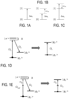
- Integration of spin qubits in silicon with photonic interfaces for long-distance quantum communication, enabling efficient quantum state transfer between stationary qubits and flying photonic qubits.
- Coherent control of electron spin states in silicon quantum dots with long coherence times, making them suitable as quantum memory nodes in distributed quantum networks.
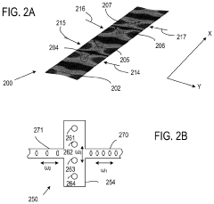
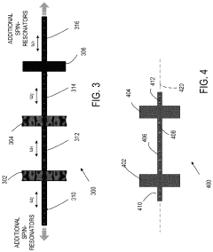
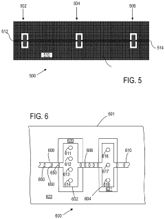
- Scalable fabrication of silicon spin qubit arrays using CMOS-compatible processes, enabling integration with classical control electronics on the same chip for quantum network nodes.
Quantum Network Security and Cryptography Implications
The integration of spin qubits in silicon into quantum networks introduces profound implications for security and cryptography. Quantum networks leveraging silicon spin qubits can potentially revolutionize secure communications through quantum key distribution (QKD) protocols, which offer theoretically unbreakable encryption based on quantum mechanical principles rather than computational complexity.
Silicon spin qubits provide unique advantages for quantum network security due to their long coherence times and compatibility with existing semiconductor manufacturing infrastructure. This combination enables the development of scalable, fault-tolerant quantum repeaters—critical components for extending quantum networks over long distances while maintaining security guarantees.
The cryptographic landscape faces significant disruption as quantum networks mature. Current public-key cryptography systems (RSA, ECC) will become vulnerable to quantum attacks, necessitating transition to quantum-resistant algorithms. Silicon spin qubit-based networks could accelerate this transition by providing platforms for testing post-quantum cryptographic protocols under realistic conditions.
Quantum networks incorporating silicon spin qubits also enable advanced security primitives beyond traditional cryptography. Secure multi-party computation, quantum digital signatures, and quantum-enhanced authentication mechanisms become feasible, offering security guarantees impossible with classical systems. These capabilities could transform financial transactions, digital identity verification, and secure access control systems.
For enterprise applications, silicon spin qubit networks present opportunities for secure distributed quantum computing—allowing organizations to process sensitive data with quantum speedup while maintaining strict security boundaries. This capability addresses a critical concern in quantum computing adoption: balancing computational advantage against data protection requirements.
The standardization of quantum network security protocols involving silicon spin qubits remains an evolving challenge. International bodies like NIST, ETSI, and ISO are developing frameworks that will determine how these technologies integrate into existing security infrastructures. Early research suggests silicon-based implementations may offer advantages in certification and validation processes due to their manufacturing consistency.
Hybrid security architectures—combining classical and quantum techniques—represent the most promising near-term approach. Silicon spin qubits could serve as quantum security accelerators within predominantly classical networks, providing quantum advantage for specific security-critical functions while leveraging established security practices for system-wide protection.
Scalability and Manufacturing Considerations
The scalability of silicon spin qubits represents a significant advantage in quantum network development. Silicon's compatibility with existing CMOS manufacturing infrastructure enables potential mass production of quantum devices using well-established fabrication techniques. This manufacturing synergy offers a clear pathway to scale from individual qubits to integrated quantum processors containing thousands or millions of qubits - a critical requirement for practical quantum networks.
Current fabrication processes for silicon spin qubits leverage advanced lithography techniques that can achieve feature sizes below 10nm. These processes allow for precise placement of dopant atoms and gate structures necessary for qubit operation. The semiconductor industry's decades of experience with silicon manufacturing provides a substantial knowledge base for addressing yield, reliability, and quality control challenges that inevitably arise during scaling efforts.
Integration density represents another crucial consideration. Silicon spin qubits typically occupy physical footprints of approximately 100nm × 100nm, significantly smaller than many competing qubit technologies. This compact size facilitates higher qubit densities on a single chip, potentially enabling more complex quantum network nodes within constrained physical spaces.
Thermal management becomes increasingly critical as qubit counts rise. While silicon spin qubits operate at extremely low temperatures (typically below 100mK), the control electronics generate heat that must be efficiently dissipated. Advanced cooling systems and thermal isolation techniques are being developed to address this challenge, with promising approaches including on-chip thermal management structures and optimized refrigeration systems.
Interconnect technologies present both challenges and opportunities for silicon spin qubit networks. Developing reliable methods to connect multiple qubit chips while maintaining quantum coherence remains an active research area. Proposed solutions include optical interconnects, superconducting transmission lines, and novel 3D integration techniques that could enable modular scaling of quantum networks.
Manufacturing variability poses a significant challenge, as quantum operations are highly sensitive to atomic-level defects and variations. Adaptive calibration techniques and error correction protocols are being developed to compensate for manufacturing imperfections, potentially allowing quantum networks to function despite inevitable fabrication variations.
The economic aspects of scaling silicon spin qubit technology also merit consideration. The ability to leverage existing semiconductor manufacturing infrastructure potentially reduces capital investment requirements compared to more exotic qubit technologies, potentially accelerating commercial deployment of quantum networks based on silicon platforms.
Unlock deeper insights with Patsnap Eureka Quick Research — get a full tech report to explore trends and direct your research. Try now!
Generate Your Research Report Instantly with AI Agent
Supercharge your innovation with Patsnap Eureka AI Agent Platform!