

Why Silicon is Preferred for Spin Qubit Implementation
OCT 11, 20259 MIN READ
Generate Your Research Report Instantly with AI Agent
Patsnap Eureka helps you evaluate technical feasibility & market potential.
Silicon Spin Qubit Evolution and Research Objectives
Quantum computing has evolved significantly since its theoretical conception in the early 1980s, with silicon spin qubits emerging as one of the most promising implementations for scalable quantum processors. The journey of silicon-based quantum computing began in the late 1990s when Bruce Kane proposed using nuclear spins of phosphorus donors in silicon as qubits. This groundbreaking proposal leveraged the semiconductor industry's existing infrastructure and manufacturing capabilities, setting the stage for silicon's prominent role in quantum computing.
The evolution of silicon spin qubits has been marked by several significant milestones. In 2012, researchers demonstrated the first single-atom spin qubit in silicon, proving the feasibility of Kane's original concept. By 2014, coherence times exceeding seconds were achieved in isotopically purified silicon, highlighting the material's exceptional quantum properties. The following years saw rapid advancements in multi-qubit operations, with two-qubit gates demonstrated by 2015 and fidelities steadily improving thereafter.
Silicon's prominence in spin qubit implementation stems from several inherent advantages. The semiconductor possesses an indirect bandgap and can be isotopically purified to nearly eliminate nuclear spins, resulting in exceptionally long coherence times for electron spins. Additionally, silicon's valley degeneracy provides an additional degree of freedom for qubit encoding, offering unique opportunities for quantum information processing not available in other materials.
The semiconductor industry's decades of experience with silicon manufacturing represents another crucial advantage. The ability to leverage existing CMOS fabrication techniques potentially enables the integration of quantum and classical components on the same chip, addressing one of the major challenges in scaling quantum computers. This manufacturing maturity also suggests pathways toward the production of large qubit arrays with high uniformity and yield.
Current research objectives in silicon spin qubits focus on several key areas. Improving qubit fidelity remains paramount, with efforts directed toward better control of the semiconductor-oxide interface and reduction of charge noise. Scaling beyond proof-of-concept devices to arrays containing hundreds or thousands of qubits represents another critical goal, requiring innovations in qubit addressing, control line routing, and cross-talk mitigation.
The development of robust error correction protocols specifically tailored to silicon's unique error mechanisms constitutes another important research direction. Additionally, researchers are exploring hybrid approaches that combine silicon spin qubits with superconducting resonators or photonic components to enable long-distance entanglement, addressing connectivity limitations inherent to nearest-neighbor coupling schemes.
The ultimate objective remains the realization of fault-tolerant quantum computation in silicon platforms, requiring continued improvements in qubit performance, control electronics, and system integration. With its combination of excellent quantum properties and manufacturing scalability, silicon continues to be a leading contender in the race toward practical quantum computing technologies.
Market Analysis for Silicon-Based Quantum Computing
The silicon-based quantum computing market is experiencing significant growth, driven by the inherent advantages silicon offers for spin qubit implementation. Current market projections indicate the global quantum computing market will reach approximately $1.7 billion by 2026, with silicon-based approaches capturing an increasing share due to their scalability and compatibility with existing semiconductor infrastructure.
Market demand for silicon-based quantum computing solutions stems primarily from sectors requiring complex computational capabilities, including pharmaceuticals, materials science, financial services, and cryptography. Pharmaceutical companies are particularly interested in quantum computing for drug discovery and molecular modeling, potentially reducing R&D timelines by 30-40% compared to traditional computing methods.
Financial institutions represent another major market segment, with quantum algorithms promising to revolutionize portfolio optimization, risk assessment, and fraud detection. Several major banks have already established quantum computing research partnerships, indicating strong commercial interest in silicon-based quantum technologies.
The market landscape features both established semiconductor giants and specialized quantum computing startups. Intel, IBM, and Samsung have made substantial investments in silicon-based quantum computing research, leveraging their existing semiconductor manufacturing expertise. Meanwhile, specialized players like Silicon Quantum Computing, Quantum Motion, and Equal1 are focusing exclusively on silicon qubit technologies.
Geographically, North America currently leads the market with approximately 45% share, followed by Europe and Asia-Pacific. However, Asia-Pacific is expected to demonstrate the highest growth rate over the next five years due to increasing government investments and strong semiconductor manufacturing capabilities, particularly in countries like Japan, China, and South Korea.
Investor interest in silicon-based quantum computing has grown substantially, with venture capital funding increasing by over 200% between 2018 and 2022. This reflects confidence in silicon's potential to deliver commercially viable quantum computers faster than competing technologies like superconducting qubits or trapped ions.
Market adoption faces several challenges, including the need for error correction, operating temperature requirements, and coherence time limitations. However, recent breakthroughs in silicon qubit fidelity and control systems have accelerated commercialization timelines. Industry analysts now predict the first commercially viable silicon-based quantum computers with practical applications could reach the market within 5-7 years.
Customer demand is increasingly focused on quantum computing as a service (QCaaS) rather than hardware ownership, creating opportunities for cloud-based quantum computing platforms that incorporate silicon-based quantum processors. This service-oriented approach is expected to dominate the initial commercialization phase, lowering barriers to entry for end-users across various industries.
Current Challenges in Silicon Spin Qubit Technology
Despite significant progress in silicon spin qubit technology, several critical challenges continue to impede its full-scale implementation and commercialization. One of the most persistent issues is the coherence time limitation. While silicon provides relatively long coherence times compared to other materials, current implementations still struggle to maintain quantum states long enough for complex quantum algorithms, with typical T2 times ranging from microseconds to milliseconds depending on the specific implementation.
Qubit fidelity remains another significant hurdle. Current silicon spin qubits demonstrate single-qubit gate fidelities around 99.9% and two-qubit gate fidelities between 98-99%, which falls short of the threshold required for fault-tolerant quantum computing, estimated at 99.99% or higher. This fidelity gap necessitates substantial improvements in control electronics, pulse shaping, and dynamical decoupling techniques.
Scalability presents perhaps the most formidable challenge. While silicon's compatibility with CMOS manufacturing processes offers theoretical advantages, practical implementation of large qubit arrays faces numerous obstacles. Current fabrication techniques struggle with consistent qubit-to-qubit coupling, precise dopant placement, and uniform electrical characteristics across larger arrays. Most advanced silicon spin qubit systems currently operate with fewer than 10 qubits, far from the millions required for practical quantum advantage.
The integration of control electronics with qubit arrays introduces another layer of complexity. The dense wiring required for individual qubit control creates significant heat dissipation issues and crosstalk problems. Current architectures typically require one or more control lines per qubit, making scaling beyond a few dozen qubits extremely challenging with conventional approaches.
Temperature dependence also remains problematic. While silicon spin qubits can operate at higher temperatures (1-4K) than superconducting qubits, they still require sophisticated cryogenic systems. The development of control electronics that can function reliably at these temperatures without generating excessive heat represents a significant engineering challenge.
Variability between qubits constitutes another major obstacle. Manufacturing inconsistencies lead to different qubit characteristics across the array, requiring individual calibration and characterization. This "qubit individuality" complicates the implementation of quantum error correction codes and scalable control systems.
Finally, the readout speed and fidelity of silicon spin qubits lag behind other quantum computing platforms. Current readout mechanisms often require integration with charge sensors or resonators, adding complexity to the system architecture and potentially limiting the speed of quantum algorithms.
Silicon-Based Spin Qubit Architectures
01 Silicon-based semiconductor manufacturing processes
Silicon is widely used in semiconductor manufacturing due to its excellent electrical properties. Various processes have been developed to create silicon-based semiconductor devices, including deposition techniques, etching methods, and doping procedures. These processes are essential for fabricating integrated circuits, transistors, and other electronic components that form the foundation of modern electronics.- Silicon-based semiconductor manufacturing processes: Silicon is widely used in semiconductor manufacturing for creating integrated circuits and electronic devices. The manufacturing processes involve techniques such as chemical vapor deposition, etching, and doping to create silicon-based transistors and other semiconductor components. These processes are fundamental to modern electronics and computing technologies, enabling the production of increasingly miniaturized and efficient electronic devices.
- Silicon materials for solar cell applications: Silicon is a primary material used in photovoltaic technology for converting sunlight into electricity. Various forms of silicon, including monocrystalline, polycrystalline, and amorphous silicon, are used in solar cell manufacturing. The processing techniques involve purification of silicon, crystal growth, wafer slicing, and surface treatments to enhance light absorption and electrical conductivity, improving the overall efficiency of solar energy conversion.
- Silicon-based materials for energy storage: Silicon materials are increasingly being utilized in energy storage applications, particularly in lithium-ion batteries. Silicon anodes offer significantly higher theoretical capacity compared to traditional graphite anodes. Various approaches to overcome challenges such as volume expansion during charging/discharging cycles include nanostructuring silicon, creating silicon-carbon composites, and developing novel silicon alloys to improve cycle life and stability of energy storage devices.
- Silicon production and purification methods: The production and purification of silicon involves multiple processes to convert raw silicon dioxide (silica) into high-purity silicon suitable for various applications. These methods include carbothermic reduction of silica, followed by various purification techniques such as the Siemens process, zone refining, and chemical vapor deposition. Advanced purification methods aim to achieve the ultra-high purity levels required for semiconductor and photovoltaic applications while reducing energy consumption and environmental impact.
- Silicon-based composite materials: Silicon is incorporated into various composite materials to enhance their properties for specific applications. These composites include silicon-polymer blends, silicon-ceramic materials, and silicon-metal alloys. The addition of silicon can improve mechanical strength, thermal stability, electrical properties, and chemical resistance. These composite materials find applications in aerospace, automotive, construction, and electronic industries, offering advantages over traditional materials in terms of performance and durability.
02 Silicon material production and purification
Methods for producing and purifying silicon materials are crucial for various industrial applications. These processes involve extracting silicon from raw materials, refining it to remove impurities, and processing it into forms suitable for specific applications. Advanced purification techniques ensure that silicon meets the high purity requirements needed for electronics, solar cells, and other high-tech applications.Expand Specific Solutions03 Silicon-based solar cell technology
Silicon is a primary material in photovoltaic technology. Innovations in silicon-based solar cells focus on improving efficiency, reducing production costs, and enhancing durability. These advancements include novel cell structures, improved manufacturing processes, and integration of silicon with other materials to optimize light absorption and energy conversion.Expand Specific Solutions04 Silicon compounds and composites
Silicon can be combined with various elements to form compounds and composites with unique properties. These materials include silicones, silicon carbide, silicon nitride, and silicon-based polymers. Such compounds find applications in diverse fields including electronics, construction, automotive, medical devices, and consumer products due to their thermal stability, electrical insulation properties, and mechanical strength.Expand Specific Solutions05 Silicon in energy storage applications
Silicon has emerged as a promising material for energy storage applications, particularly in battery technology. Silicon-based anodes can significantly increase the capacity of lithium-ion batteries compared to traditional graphite anodes. Research focuses on overcoming challenges related to silicon's volume expansion during charging cycles, improving cycle life, and enhancing overall battery performance through novel silicon structures and composites.Expand Specific Solutions
Leading Organizations in Silicon Quantum Computing
Silicon's dominance in spin qubit implementation reflects the quantum computing industry's early growth phase, with an estimated market size of $500-700 million and rapidly expanding. The technology is transitioning from research to early commercialization, with varying maturity levels across key players. Companies like IBM, GlobalFoundries, and Intel leverage silicon's compatibility with existing semiconductor infrastructure, while research institutions such as CEA, IMEC, and MIT focus on overcoming coherence challenges. Origin Quantum and D-Wave represent emerging competitors exploring alternative approaches. Silicon's scalability advantages and integration with CMOS technology position it as the preferred material despite competition from other qubit implementations, creating a competitive landscape balanced between established semiconductor giants and specialized quantum startups.
GlobalFoundries U.S., Inc.
Technical Solution: GlobalFoundries has developed a specialized silicon fabrication process tailored for quantum computing applications, particularly for spin qubit implementation. Their approach leverages their 22FDX platform, which provides fully-depleted silicon-on-insulator (FDSOI) technology with exceptional electrostatic control at the nanoscale level required for quantum dot formation. GlobalFoundries' process enables the creation of high-quality, uniform quantum dots with minimal variability across wafers, addressing one of the key challenges in scaling silicon spin qubits. Their technology incorporates specialized implantation techniques to precisely position dopants for deterministic single-electron confinement. The company has established dedicated fabrication lines with ultra-clean processing to minimize impurities that could degrade coherence times. GlobalFoundries has also developed specialized metallization schemes compatible with cryogenic operation, ensuring reliable electrical contacts to quantum devices at millikelvin temperatures[3]. Their process includes integration capabilities for on-chip control electronics, moving toward a more scalable quantum computing architecture.
Strengths: Industry-leading semiconductor manufacturing capabilities ensure high yield and reproducibility of quantum devices. Their established supply chain and quality control systems provide advantages for eventual commercialization. Weaknesses: As primarily a manufacturing partner, GlobalFoundries depends on design partners for quantum architecture innovations, potentially limiting their ability to drive fundamental breakthroughs in qubit design independently.
Interuniversitair Micro-Electronica Centrum VZW
Technical Solution: IMEC has developed an advanced silicon spin qubit platform that leverages their expertise in semiconductor process technology. Their approach focuses on creating highly uniform silicon quantum dots using 300mm wafer processing techniques compatible with industrial manufacturing. IMEC's silicon spin qubit implementation utilizes a multi-layer gate stack architecture that enables precise electrostatic control of individual electrons in quantum dots. They have pioneered the use of silicon-germanium (SiGe) heterostructures to create strain-engineered quantum wells that enhance electron mobility and improve qubit performance. IMEC's process incorporates specialized deposition techniques for creating ultra-thin, high-quality gate dielectrics that minimize charge noise and improve qubit coherence times. Their technology includes integrated sensors for single-shot readout of spin states with high fidelity. IMEC has demonstrated the ability to fabricate arrays of quantum dots with controllable tunnel coupling between adjacent sites, a critical requirement for two-qubit operations[4]. Their platform includes specialized interconnect solutions designed to minimize thermal loads while maintaining signal integrity at cryogenic temperatures, addressing one of the key challenges in scaling silicon spin qubit systems.
Strengths: Exceptional process control capabilities enable the creation of highly uniform quantum devices across entire wafers. Their established partnerships with leading semiconductor equipment manufacturers facilitate rapid technology transfer to production environments. Weaknesses: The complex heterostructure approach may introduce additional fabrication challenges and potential material interface issues that could affect qubit performance and yield at scale.
Key Patents and Breakthroughs in Silicon Spin Qubits
A qubit device and a method for operating a qubit device
PatentPendingEP3967650A1
Innovation
- A qubit device with a semiconductor substrate and nanomagnets arranged above electrostatically confined quantum dots, where every other quantum dot is subjected to an out-of-plane magnetic field, allowing for selective qubit control and resonance frequency shifting, thereby enabling scalable and efficient qubit systems with reduced spin-orbit coupling.


Silicon single electron device
PatentActiveUS20090309229A1
Innovation
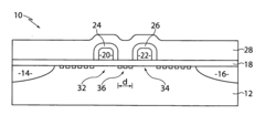
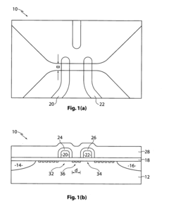
- A silicon integrated circuit device with ohmic contact regions, insulating layers, and tunable aluminium gates is developed, allowing for the creation of quantum dots and single-electron transistors (SETs) that can confine electrons and control charge flow, enabling sensitive electrometry and operation at radio frequencies.
Material Science Considerations for Quantum Computing
Silicon has emerged as the preferred material for spin qubit implementation in quantum computing due to its exceptional material properties and compatibility with existing semiconductor manufacturing infrastructure. The crystalline structure of silicon provides an ideal environment for electron spin qubits, offering long coherence times that are essential for quantum operations. High-purity silicon, particularly isotopically enriched silicon-28, significantly reduces spin-orbit coupling and hyperfine interactions that typically cause decoherence in quantum systems.
The semiconductor industry's decades of experience with silicon fabrication presents a substantial advantage for scaling quantum technologies. Established CMOS (Complementary Metal-Oxide-Semiconductor) manufacturing processes can be leveraged to produce silicon-based quantum devices with nanometer precision, enabling the integration of quantum and classical components on the same chip. This manufacturing maturity translates to higher yield rates and more consistent device performance compared to alternative materials.
Silicon's band structure and electronic properties offer additional benefits for quantum computing applications. The presence of multiple conduction band valleys in silicon allows for valley splitting, which can be exploited for qubit manipulation and control. Furthermore, the relatively large effective mass of electrons in silicon reduces their susceptibility to environmental noise, enhancing qubit stability.
The thermal properties of silicon also contribute to its suitability for quantum computing implementations. Silicon's high thermal conductivity facilitates efficient heat dissipation, which is crucial for maintaining the ultra-low temperatures required for quantum operations. This characteristic becomes increasingly important as quantum systems scale to include more qubits and control electronics.
Recent advancements in silicon purification techniques have further enhanced its viability for quantum applications. Modern methods can achieve silicon with 99.99999% purity, minimizing the presence of paramagnetic impurities that could disrupt quantum states. Additionally, precise doping techniques allow for controlled introduction of phosphorus or other donor atoms that serve as qubit hosts within the silicon lattice.
The interface between silicon and silicon dioxide (SiO2) provides excellent electrical isolation properties, enabling the creation of well-defined quantum dots with minimal leakage currents. This characteristic is particularly valuable for gate-defined quantum dots, where electrostatic control of individual electrons is essential for qubit manipulation.
Quantum Error Correction in Silicon Systems
Quantum Error Correction in Silicon Systems represents a critical frontier in advancing silicon-based quantum computing toward practical applications. Silicon spin qubits inherently offer longer coherence times compared to many competing platforms, providing a natural advantage for error correction schemes. However, even with these favorable properties, quantum error correction remains essential for achieving fault-tolerant quantum computation.
The surface code architecture has emerged as a particularly promising approach for silicon-based systems. This error correction protocol arranges physical qubits in a two-dimensional lattice, where data qubits store quantum information while measurement qubits detect errors. Silicon's ability to host densely packed qubits with high fidelity control makes it well-suited for implementing such complex error correction codes.
Recent experimental demonstrations have shown significant progress in implementing basic error correction primitives in silicon. These include the realization of small-scale error detection circuits and the demonstration of high-fidelity two-qubit gates necessary for syndrome extraction. The compatibility of silicon fabrication with existing CMOS technology has enabled the integration of classical control electronics alongside quantum devices, facilitating the rapid measurement and feedback operations crucial for error correction.
One distinctive advantage of silicon systems for quantum error correction is the potential for isotopic purification. Natural silicon contains approximately 4.7% of 29Si isotopes, which possess nuclear spins that can cause decoherence. Isotopically purified silicon (28Si) substantially reduces this noise source, extending coherence times and lowering the physical error rates, thereby reducing the overhead required for effective error correction.
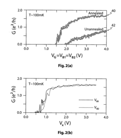
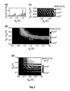
Challenges remain in scaling silicon-based error correction to the threshold required for fault tolerance. Current estimates suggest that physical error rates must be reduced to approximately 10^-3 or lower for practical error correction. While silicon spin qubits have demonstrated single-qubit gate fidelities exceeding 99.9%, two-qubit operations typically exhibit higher error rates that must be improved.
Looking forward, hybrid approaches combining silicon's long coherence times with complementary quantum systems for specific operations may offer novel pathways to effective error correction. Additionally, tailored error correction codes that exploit the specific noise characteristics of silicon spin systems could potentially reduce resource requirements compared to generic approaches.
The surface code architecture has emerged as a particularly promising approach for silicon-based systems. This error correction protocol arranges physical qubits in a two-dimensional lattice, where data qubits store quantum information while measurement qubits detect errors. Silicon's ability to host densely packed qubits with high fidelity control makes it well-suited for implementing such complex error correction codes.
Recent experimental demonstrations have shown significant progress in implementing basic error correction primitives in silicon. These include the realization of small-scale error detection circuits and the demonstration of high-fidelity two-qubit gates necessary for syndrome extraction. The compatibility of silicon fabrication with existing CMOS technology has enabled the integration of classical control electronics alongside quantum devices, facilitating the rapid measurement and feedback operations crucial for error correction.
One distinctive advantage of silicon systems for quantum error correction is the potential for isotopic purification. Natural silicon contains approximately 4.7% of 29Si isotopes, which possess nuclear spins that can cause decoherence. Isotopically purified silicon (28Si) substantially reduces this noise source, extending coherence times and lowering the physical error rates, thereby reducing the overhead required for effective error correction.
Challenges remain in scaling silicon-based error correction to the threshold required for fault tolerance. Current estimates suggest that physical error rates must be reduced to approximately 10^-3 or lower for practical error correction. While silicon spin qubits have demonstrated single-qubit gate fidelities exceeding 99.9%, two-qubit operations typically exhibit higher error rates that must be improved.
Looking forward, hybrid approaches combining silicon's long coherence times with complementary quantum systems for specific operations may offer novel pathways to effective error correction. Additionally, tailored error correction codes that exploit the specific noise characteristics of silicon spin systems could potentially reduce resource requirements compared to generic approaches.
Unlock deeper insights with Patsnap Eureka Quick Research — get a full tech report to explore trends and direct your research. Try now!
Generate Your Research Report Instantly with AI Agent
Supercharge your innovation with Patsnap Eureka AI Agent Platform!