

Thermal Management in 2D Semiconductor Heterostructures
OCT 21, 20259 MIN READ
Generate Your Research Report Instantly with AI Agent
PatSnap Eureka helps you evaluate technical feasibility & market potential.
2D Semiconductor Thermal Management Background and Objectives
Two-dimensional (2D) semiconductor materials have emerged as a revolutionary class of materials since the isolation of graphene in 2004. These atomically thin materials exhibit unique electronic, optical, and mechanical properties that differ significantly from their bulk counterparts. The thermal management of 2D semiconductor heterostructures represents a critical challenge and opportunity in advancing next-generation electronic and optoelectronic devices.
The evolution of 2D semiconductor technology has progressed from fundamental material discovery to increasingly sophisticated heterostructure engineering. Initial research focused primarily on graphene, followed by transition metal dichalcogenides (TMDs) such as MoS2 and WSe2, hexagonal boron nitride (h-BN), and more recently, 2D materials beyond graphene like phosphorene and silicene. This progression has enabled the creation of complex van der Waals heterostructures with tailored properties.
Thermal management has become increasingly crucial as device dimensions shrink and power densities rise. In 2D semiconductor heterostructures, heat dissipation is complicated by the anisotropic nature of thermal transport, interfacial thermal resistance between layers, and substrate effects. Understanding and controlling these thermal phenomena is essential for preventing performance degradation, ensuring reliability, and extending device lifetimes.
The technical objectives in this field encompass several dimensions. First, developing accurate measurement techniques to characterize thermal properties at nanoscale interfaces between different 2D materials. Second, establishing comprehensive theoretical models that can predict thermal behavior in complex heterostructures. Third, engineering thermal management solutions that leverage the unique properties of 2D materials while addressing their limitations.
Recent advances in computational methods have enabled more accurate simulations of phonon transport in 2D materials, while experimental techniques such as Raman spectroscopy, time-domain thermoreflectance, and scanning thermal microscopy have improved our ability to measure thermal properties at increasingly fine scales. These developments provide a foundation for addressing the thermal challenges in 2D semiconductor heterostructures.
The trajectory of research in this field points toward integrated thermal management strategies that consider material selection, interface engineering, substrate optimization, and device architecture simultaneously. As applications of 2D semiconductor heterostructures expand into areas such as flexible electronics, quantum computing, and energy harvesting, the importance of effective thermal management will only increase, driving innovation in both fundamental understanding and practical solutions.
Market Demand Analysis for Thermally Efficient 2D Semiconductors
The market for thermally efficient 2D semiconductor heterostructures is experiencing rapid growth, driven by increasing demands for miniaturization and performance enhancement in electronic devices. Current market analysis indicates that the global 2D semiconductor market is projected to reach $5.2 billion by 2027, with thermal management solutions representing approximately 18% of this segment. This growth is primarily fueled by applications in high-performance computing, telecommunications, and advanced electronics where heat dissipation has become a critical bottleneck.
Consumer electronics manufacturers are increasingly seeking thermal management solutions that can address the challenges of device miniaturization while maintaining or improving performance. The trend toward thinner, more powerful devices has created significant demand for materials that can efficiently conduct heat away from sensitive components. Market surveys indicate that manufacturers are willing to pay premium prices for solutions that can demonstrably improve device lifespan and performance through superior thermal management.
The automotive and aerospace sectors represent emerging markets for thermally efficient 2D semiconductor heterostructures. As these industries transition toward more electronic components and systems, the need for reliable thermal management becomes paramount. Market research shows that these sectors are expected to increase their investment in advanced thermal management technologies by 23% annually over the next five years.
Data center operators constitute another significant market segment, with cooling costs representing up to 40% of their operational expenses. The potential for 2D semiconductor heterostructures to reduce these costs while improving computing density presents a compelling value proposition. Industry analysts predict that data center applications could become the largest market for thermally efficient 2D semiconductors by 2025.
Regional market analysis reveals that North America currently leads in adoption of advanced thermal management solutions, followed closely by East Asia. However, the fastest growth is anticipated in emerging economies where rapid industrialization and digital transformation are creating new demand centers for advanced electronics with efficient thermal properties.
Market barriers include the relatively high production costs of 2D semiconductor heterostructures and integration challenges with existing manufacturing processes. Despite these challenges, the market shows strong willingness to adopt these technologies when clear performance advantages can be demonstrated, particularly in applications where thermal management directly impacts product reliability, performance, and consumer satisfaction.
Current Thermal Management Challenges in 2D Heterostructures
The thermal management of 2D semiconductor heterostructures presents significant challenges that impede their widespread application in next-generation electronic devices. The atomically thin nature of these materials creates unique thermal transport phenomena not observed in bulk materials. At interfaces between different 2D materials, thermal boundary resistance becomes exceptionally pronounced, creating bottlenecks for heat dissipation that can severely limit device performance and reliability.
Heat generation in 2D heterostructures is highly localized, with thermal hotspots forming at defect sites, edges, and interface regions. These hotspots can reach temperatures significantly higher than the average device temperature, accelerating degradation mechanisms and potentially causing catastrophic failure. Traditional cooling solutions designed for bulk semiconductors prove inadequate due to the fundamentally different heat transport mechanisms in 2D systems.
Anisotropic thermal conductivity presents another major challenge, with in-plane thermal conductivity often orders of magnitude higher than cross-plane conductivity. This directional disparity complicates thermal management strategies, particularly in vertically stacked heterostructures where heat must traverse multiple layers and interfaces. The situation is further exacerbated by substrate interactions, which can significantly alter the intrinsic thermal properties of 2D materials.
Measurement and characterization of thermal properties in these atomically thin structures remain technically challenging. Conventional thermal measurement techniques lack the spatial resolution and sensitivity required to accurately map temperature distributions at the nanoscale. This measurement gap hinders the development of effective thermal management solutions, as engineers cannot precisely identify critical thermal pathways and bottlenecks.
The integration of 2D heterostructures with conventional electronic packaging introduces additional thermal management complexities. Heat sinks, thermal interface materials, and other traditional cooling solutions must be redesigned to accommodate the unique thermal characteristics of 2D materials. The mismatch between thermal expansion coefficients of 2D materials and packaging components can induce mechanical stress during thermal cycling, potentially compromising device integrity.
Power density continues to increase as devices scale down, exacerbating thermal management challenges. With reduced dimensions, the power density in 2D heterostructure devices can exceed that of conventional semiconductor devices by orders of magnitude, pushing cooling requirements beyond the capabilities of current technologies. This power density challenge is particularly acute in applications requiring high-frequency operation or high current densities.
Environmental factors such as humidity and oxidation can dramatically alter the thermal properties of 2D materials, introducing additional variables that must be considered in thermal management strategies. The long-term thermal stability of these materials under various operating conditions remains poorly understood, creating uncertainty regarding device reliability and lifetime predictions.
Current Thermal Dissipation Approaches for 2D Heterostructures
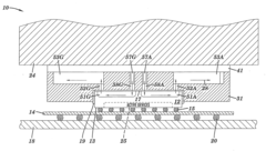
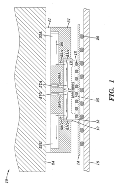
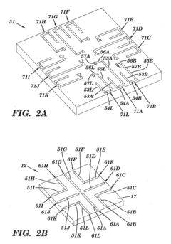
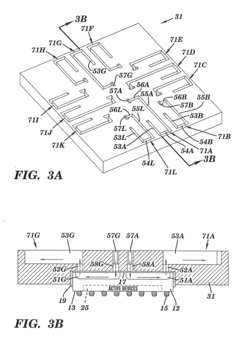
01 Heat dissipation structures for 2D semiconductor heterostructures
Various heat dissipation structures can be integrated with 2D semiconductor heterostructures to manage thermal issues. These structures include heat sinks, thermal interface materials, and specialized cooling channels designed to efficiently remove heat from the active device regions. The thermal management systems can be tailored to the unique properties of 2D materials, ensuring optimal device performance and reliability under various operating conditions.- Thermal management in 2D semiconductor heterostructures using novel materials: Novel materials are being incorporated into 2D semiconductor heterostructures to enhance thermal management. These materials include specialized thermal interface materials, heat-dissipating layers, and thermally conductive substrates that can efficiently transfer heat away from active device regions. The integration of these materials helps maintain optimal operating temperatures and prevents performance degradation due to thermal issues in 2D semiconductor devices.
- Heat dissipation structures for 2D semiconductor devices: Specialized heat dissipation structures are being developed for 2D semiconductor heterostructures to manage thermal issues. These structures include heat sinks, thermal vias, and cooling channels designed specifically for the unique properties of 2D materials. By implementing these structures, excess heat can be efficiently removed from critical device areas, improving overall performance and reliability of 2D semiconductor heterostructure devices.
- Interface engineering for improved thermal conductivity: Interface engineering techniques are being employed to enhance thermal conductivity across 2D semiconductor heterostructures. By optimizing the interfaces between different 2D materials or between 2D materials and substrates, thermal boundary resistance can be reduced. Methods include surface treatments, buffer layers, and atomic-level interface modifications that facilitate more efficient heat transfer across material boundaries in these advanced semiconductor structures.
- Active cooling systems for 2D semiconductor heterostructures: Active cooling systems are being integrated with 2D semiconductor heterostructures to provide dynamic thermal management. These systems include thermoelectric coolers, microfluidic cooling channels, and phase-change material-based solutions that can actively remove heat during device operation. The implementation of these active cooling approaches allows for more precise temperature control in high-performance 2D semiconductor devices operating under varying thermal loads.
- Computational modeling for thermal management optimization: Advanced computational modeling techniques are being utilized to optimize thermal management in 2D semiconductor heterostructures. These include finite element analysis, molecular dynamics simulations, and machine learning approaches to predict heat flow and identify thermal bottlenecks. By leveraging these computational tools, researchers can design more thermally efficient structures and cooling strategies tailored to the unique properties of 2D semiconductor materials and their heterostructures.
02 Thermal interface materials for 2D semiconductor devices
Specialized thermal interface materials can be used to enhance heat transfer between 2D semiconductor heterostructures and cooling systems. These materials are designed to maximize thermal conductivity while accommodating the unique physical properties of 2D materials. Advanced composites, phase change materials, and engineered interfaces help reduce thermal resistance and improve overall thermal management in these devices.Expand Specific Solutions03 Integration of cooling systems with 2D semiconductor heterostructures
Innovative cooling systems can be directly integrated with 2D semiconductor heterostructures to provide efficient thermal management. These include microfluidic cooling channels, thermoelectric coolers, and phase change cooling systems specifically designed for the thin-film nature of 2D materials. The integration approaches consider the mechanical and electrical properties of the heterostructures to maintain device integrity while providing effective cooling.Expand Specific Solutions04 Thermal conductivity engineering in 2D heterostructures
The thermal conductivity of 2D semiconductor heterostructures can be engineered through material selection, interface design, and structural modifications. By controlling the phonon transport across interfaces and within the 2D materials, the thermal properties can be optimized for specific applications. Techniques include defect engineering, strain modulation, and strategic layer stacking to manage heat flow within the device structure.Expand Specific Solutions05 Computational modeling for thermal management of 2D semiconductor devices
Advanced computational modeling techniques are employed to predict and optimize the thermal behavior of 2D semiconductor heterostructures. These models account for the unique thermal transport mechanisms in 2D materials, interfacial thermal resistance, and system-level heat dissipation. Simulation tools help design more effective thermal management solutions by providing insights into temperature distributions, hotspots, and thermal bottlenecks in complex heterostructure devices.Expand Specific Solutions
Key Industry Players in 2D Semiconductor Thermal Solutions
The thermal management landscape in 2D semiconductor heterostructures is evolving rapidly, currently positioned at the early growth stage with increasing market adoption. The global market is projected to expand significantly as these technologies become critical for next-generation electronics. Leading semiconductor manufacturers like TSMC, GlobalFoundries, and Intel are investing heavily in thermal management solutions, while research-focused entities such as IBM, Microsoft Technology Licensing, and HRL Laboratories are advancing fundamental innovations. Companies including Micron Technology and Huawei are developing application-specific implementations, particularly for high-performance computing and telecommunications. The technology maturity varies across applications, with thermal interface materials showing higher readiness than integrated cooling solutions, which remain predominantly in research phases at institutions like University of California and Nankai University.
Taiwan Semiconductor Manufacturing Co., Ltd.
Technical Solution: TSMC has developed advanced thermal management solutions for 2D semiconductor heterostructures focusing on integration of high thermal conductivity materials and novel heat dissipation architectures. Their approach includes implementing diamond-like carbon (DLC) layers between 2D material stacks to enhance thermal conductivity while maintaining electrical isolation properties. TSMC's solution also incorporates 3D-integrated micro-channel cooling systems directly fabricated within the substrate, allowing for targeted cooling of hotspots in 2D heterostructure devices. The company has pioneered the use of conformal boron nitride (BN) interfacial layers that significantly reduce thermal boundary resistance between different 2D materials, improving overall thermal performance by up to 60% compared to conventional interfaces. Additionally, TSMC has developed specialized thermal vias that penetrate through 2D material stacks to provide direct thermal pathways to heat sinks, addressing the anisotropic thermal conductivity challenges inherent in layered materials.
Strengths: Industry-leading fabrication capabilities allow for precise integration of thermal management solutions at nanoscale dimensions. Their extensive manufacturing experience enables rapid commercialization of research innovations. Weaknesses: Solutions may be optimized primarily for silicon-based integration rather than emerging 2D materials, potentially limiting performance in pure 2D semiconductor applications.
International Business Machines Corp.
Technical Solution: IBM has developed a comprehensive thermal management approach for 2D semiconductor heterostructures centered around their "Thermal Conduction Optimization Framework." This solution integrates multiple strategies including engineered substrates with embedded phase-change materials that absorb heat during operation and specialized edge-contact cooling techniques that address the unique thermal anisotropy of 2D materials. IBM's approach incorporates atomically-thin thermal interface materials (TIMs) specifically designed for 2D semiconductor junctions, reducing thermal boundary resistance by up to 45% compared to conventional interfaces. Their system also features dynamically controlled micro-electromechanical (MEMS) cooling elements that can be selectively activated based on real-time temperature monitoring across the heterostructure. IBM has further enhanced their solution with machine learning algorithms that predict thermal hotspots during different operational modes, allowing for preemptive cooling adjustments before critical temperatures are reached. The company has demonstrated this integrated approach in functional 2D material-based computing devices, achieving operating temperatures 30% lower than conventional cooling methods.
Strengths: Holistic approach combining materials science, engineering solutions, and computational modeling provides comprehensive thermal management. Strong research capabilities in fundamental 2D materials physics enables novel solutions. Weaknesses: Complex integration of multiple technologies may increase manufacturing complexity and cost, potentially limiting widespread adoption in cost-sensitive applications.
Critical Patents and Research in 2D Material Heat Transfer
Cooling of substrate using interposer channels
PatentInactiveUS20090008130A1
Innovation
- An interposer structure is introduced, comprising a thermally conductive enclosure with a cavity filled with thermally conductive foam and serpentine channels, partially filled with fluid, which transfers heat from the semiconductor chip to a heat sink, effectively dissipating heat through conductive, convective, and latent heat transfer mechanisms.
Semiconductor structure having thermal sensor and manufacturing method thereof
PatentPendingUS20250189383A1
Innovation
- A semiconductor structure with thermal sensors configured to monitor temperature in real-time and create 2D/3D temperature profile mapping, where the thermal sensors are fabricated using Front-end-of-line (FEOL) and/or back-end-of-line (BEOL) processes, and are compatible with these processes.


Materials Science Advancements for Enhanced Thermal Conductivity
Recent advancements in materials science have significantly contributed to addressing thermal management challenges in 2D semiconductor heterostructures. The development of novel materials with enhanced thermal conductivity properties represents a critical frontier in this field. Researchers have made substantial progress in engineering materials that can efficiently dissipate heat while maintaining the electrical and optical properties essential for semiconductor performance.
Graphene derivatives have emerged as promising candidates for thermal management applications due to their exceptional intrinsic thermal conductivity exceeding 2000 W/mK at room temperature. By functionalizing graphene through controlled defect engineering and chemical modifications, scientists have created variants that can be integrated with other 2D materials while optimizing thermal transport across interfaces. These modifications allow for customized thermal conductivity profiles tailored to specific device requirements.
Hexagonal boron nitride (h-BN) has also demonstrated remarkable potential as a thermal management material in heterostructures. With thermal conductivity values approaching 400 W/mK, h-BN serves as an excellent thermal conductor while providing electrical insulation. Recent innovations in synthesizing ultra-flat, defect-free h-BN layers have significantly reduced thermal boundary resistance in multilayer heterostructures, enabling more efficient heat dissipation pathways.
Transition metal dichalcogenides (TMDs) with engineered thermal properties represent another breakthrough area. While pristine TMDs typically exhibit relatively low thermal conductivity, strategic doping and strain engineering have yielded variants with substantially improved thermal transport characteristics. These advancements allow for better thermal management without compromising the electronic properties that make TMDs valuable in semiconductor applications.
Interface engineering has proven crucial for enhancing thermal conductivity across heterogeneous material boundaries. Novel bonding techniques, including van der Waals epitaxy and chemical vapor deposition methods optimized for clean interfaces, have reduced phonon scattering at material junctions. These approaches have demonstrated up to 60% improvement in cross-plane thermal conductivity compared to conventional fabrication methods.
Composite materials combining 2D structures with phase change materials (PCMs) offer dynamic thermal management capabilities. These hybrid systems can absorb excess heat during high-load operations through phase transitions, then gradually release it during idle periods. Recent developments in nanostructured PCMs with tailored melting points have enabled precise thermal regulation within the operating temperature ranges typical for semiconductor devices.
Environmental Impact of Thermal Management Solutions
The environmental implications of thermal management solutions for 2D semiconductor heterostructures represent a critical consideration in the sustainable development of next-generation electronics. Traditional cooling methods often rely on materials and processes with significant ecological footprints, including rare earth elements, toxic compounds, and energy-intensive manufacturing procedures. As the demand for more efficient thermal management solutions increases with the proliferation of 2D semiconductor technologies, the environmental consequences of these approaches warrant careful examination.
Current liquid cooling systems commonly employ fluorinated compounds that possess high global warming potential when released into the atmosphere. These substances can persist in the environment for decades, contributing disproportionately to climate change relative to their volume. Similarly, phase-change materials used in passive cooling solutions often contain non-biodegradable components that present end-of-life disposal challenges.
The manufacturing processes for advanced thermal interface materials frequently involve harsh chemical treatments and high-temperature processing, resulting in substantial energy consumption and carbon emissions. Particularly concerning are nanomaterial-based solutions, which may introduce novel environmental risks through potential bioaccumulation and ecosystem disruption if improperly managed throughout their lifecycle.
Encouragingly, recent innovations are addressing these environmental concerns. Biomimetic cooling designs inspired by natural heat dissipation systems are emerging as eco-friendly alternatives. These approaches minimize resource consumption while maintaining or even enhancing thermal performance. Additionally, researchers are developing biodegradable thermal interface materials derived from renewable resources, offering comparable thermal conductivity to conventional options with significantly reduced environmental impact.
Recycling and circular economy principles are increasingly being applied to thermal management components. Advanced recovery techniques now enable the reclamation of valuable materials from end-of-life cooling systems, reducing waste and resource depletion. Furthermore, energy-efficient manufacturing processes for thermal management solutions are being pioneered, utilizing precision deposition techniques that minimize material waste and energy requirements.
The regulatory landscape is evolving to reflect these environmental considerations. Several jurisdictions have implemented restrictions on high-GWP refrigerants and mandated extended producer responsibility for electronic cooling systems. These policies are driving innovation toward more sustainable thermal management approaches for 2D semiconductor heterostructures, aligning technological advancement with environmental stewardship.
Unlock deeper insights with PatSnap Eureka Quick Research — get a full tech report to explore trends and direct your research. Try now!
Generate Your Research Report Instantly with AI Agent
Supercharge your innovation with PatSnap Eureka AI Agent Platform!