Transparent Transistor Design Innovations for Sensor Technologies
OCT 21, 202510 MIN READ
Generate Your Research Report Instantly with AI Agent
PatSnap Eureka helps you evaluate technical feasibility & market potential.
Transparent Transistor Evolution and Objectives
Transparent transistors have evolved significantly since their inception in the early 2000s, transforming from laboratory curiosities to essential components in advanced sensing technologies. The journey began with zinc oxide-based thin-film transistors (TFTs), which demonstrated modest transparency but suffered from stability issues and limited performance metrics. These early iterations primarily utilized amorphous oxide semiconductors that offered optical transparency but struggled with carrier mobility limitations and manufacturing challenges at scale.
The field experienced a paradigm shift with the introduction of indium gallium zinc oxide (IGZO) transistors around 2010, which dramatically improved electron mobility while maintaining excellent transparency. This breakthrough enabled the first commercially viable transparent electronic circuits and laid the groundwork for integration with sensing applications. The subsequent development of solution-processed metal oxide semiconductors further expanded manufacturing possibilities, allowing for lower temperature deposition and compatibility with flexible substrates.
Recent years have witnessed the emergence of novel materials beyond traditional metal oxides, including carbon-based alternatives such as graphene and carbon nanotubes, which offer exceptional electrical properties alongside optical transparency. These materials have pushed the boundaries of what's possible in transparent electronics, enabling transistors with sub-nanometer channel lengths and switching speeds approaching those of conventional silicon devices.
The evolution of transparent transistor technology has been driven by several key objectives that continue to shape research directions. Primary among these is achieving the optimal balance between optical transparency and electrical performance—a fundamental challenge that requires innovative material engineering and device architecture. Researchers aim to develop transistors with transparency exceeding 90% across the visible spectrum while maintaining carrier mobilities above 10 cm²/Vs and on/off ratios greater than 10⁶.
Another critical objective is enhancing environmental stability, as many transparent semiconductor materials remain susceptible to degradation from oxygen, moisture, and light exposure. This has spurred research into encapsulation techniques and intrinsically stable material compositions that can withstand real-world operating conditions without performance deterioration.
The integration capability with existing manufacturing processes represents another pivotal goal, as commercial viability depends on compatibility with established production methods. This includes developing deposition techniques that operate at temperatures compatible with plastic substrates (<200°C) and patterning methods that achieve micron-scale resolution without compromising material properties.
For sensor technologies specifically, the objectives extend to creating transistors with high sensitivity to external stimuli such as light, pressure, temperature, or chemical species. This sensing functionality, combined with transparency, opens unprecedented possibilities for invisible electronic systems that can monitor environments without visual interference—a capability particularly valuable in medical diagnostics, environmental monitoring, and augmented reality applications.
Market Applications for Transparent Sensor Technologies
Transparent transistor technologies are rapidly transforming the sensor market landscape, creating unprecedented opportunities across multiple industries. The integration of transparent sensors into consumer electronics represents one of the most promising market segments, with applications ranging from transparent touchscreens and flexible displays to wearable health monitors. Major smartphone manufacturers are increasingly investing in transparent sensor technologies to develop next-generation devices with enhanced functionality and aesthetic appeal.
The automotive industry has emerged as another significant market for transparent sensor technologies. Advanced driver-assistance systems (ADAS) and autonomous vehicles require sophisticated sensing capabilities that can be seamlessly integrated into windshields and windows. Transparent sensors enable critical functions such as rain detection, light sensing, and even heads-up displays without obstructing the driver's view, thereby enhancing both safety and user experience.
Healthcare applications represent a high-value market segment for transparent sensor technologies. From continuous glucose monitoring systems to smart bandages that track wound healing, transparent sensors offer non-intrusive monitoring solutions that improve patient comfort and compliance. The aging global population and increasing prevalence of chronic diseases are driving substantial growth in this sector, with transparent biosensors playing a pivotal role in remote patient monitoring systems.
The smart building sector is rapidly adopting transparent sensor technologies for energy management and security applications. Transparent photovoltaic sensors integrated into windows can simultaneously harvest solar energy and monitor environmental conditions, while transparent security sensors can be inconspicuously embedded into glass surfaces. These innovations contribute to more sustainable and secure building designs without compromising architectural aesthetics.
Industrial applications of transparent sensors are expanding in manufacturing environments where traditional opaque sensors would interfere with processes or visibility. Quality control systems increasingly utilize transparent optical sensors for defect detection in production lines, while transparent gas and chemical sensors monitor workplace safety conditions without obstructing critical equipment or sightlines.
The military and aerospace sectors represent specialized but lucrative markets for transparent sensor technologies. Applications include transparent radar systems, heads-up displays for fighter pilots, and environmental monitoring sensors for spacecraft. These applications demand the highest performance standards and offer premium pricing opportunities for advanced transparent transistor technologies.
Emerging applications in augmented reality and smart cities are creating new market opportunities. Transparent sensors embedded in AR glasses enable contextual awareness and enhanced user interactions, while smart city infrastructure increasingly incorporates transparent environmental monitoring sensors into urban elements like bus shelters and information displays.
Technical Barriers in Transparent Transistor Development
Despite significant advancements in transparent transistor technology, several critical technical barriers continue to impede the full realization of their potential in sensor applications. The fundamental challenge lies in achieving the optimal balance between transparency and electrical performance. Conventional semiconductor materials with excellent electrical properties, such as silicon, are inherently opaque, while highly transparent materials often exhibit poor carrier mobility and electrical stability.
Material limitations represent a primary obstacle, as the most widely used transparent conducting oxides (TCOs) like indium tin oxide (ITO) and indium gallium zinc oxide (IGZO) face trade-offs between transparency, conductivity, and mechanical flexibility. The scarcity and rising cost of indium further complicate large-scale implementation, driving the need for alternative materials that maintain performance without relying on rare elements.
Processing challenges create another significant barrier. The deposition of uniform, defect-free transparent thin films requires precise control over processing parameters. Traditional high-temperature annealing processes used to improve crystallinity and electrical properties often damage temperature-sensitive substrates necessary for flexible applications. Low-temperature alternatives frequently result in films with higher defect densities and inferior electrical characteristics.
Interface engineering presents complex difficulties, particularly in multilayer transparent transistor structures. The formation of high-quality interfaces between different functional layers is crucial for device performance but remains challenging to achieve consistently. Charge trapping at these interfaces leads to threshold voltage instability and hysteresis effects that compromise sensor reliability and response time.
Environmental stability constitutes a persistent concern, as many transparent semiconductor materials exhibit sensitivity to ambient conditions. Exposure to oxygen, moisture, and light can significantly alter electrical properties through mechanisms such as oxygen adsorption/desorption and photoinduced carrier generation. This environmental sensitivity necessitates effective encapsulation strategies that maintain transparency while providing protection.
Scaling and integration barriers emerge when transitioning from single-device demonstrations to integrated sensor arrays. The development of compatible fabrication processes that maintain performance consistency across large areas remains challenging. Additionally, the integration of transparent transistors with other sensor components and readout circuitry introduces complex design constraints and potential compatibility issues.
Reliability and aging effects present long-term challenges, as transparent transistors often exhibit performance degradation under continuous operation or bias stress. Understanding and mitigating these degradation mechanisms is essential for developing sensors with acceptable operational lifetimes, particularly for applications requiring extended deployment periods.
Current Transparent Transistor Architectures
01 Transparent oxide semiconductor materials for transistors
Various oxide semiconductor materials can be used to create transparent transistors. These materials, such as indium gallium zinc oxide (IGZO), zinc oxide (ZnO), and other metal oxides, offer high electron mobility while maintaining optical transparency. The unique properties of these materials allow for the fabrication of transistors that can be integrated into transparent electronic devices, displays, and sensors without blocking light transmission.- Transparent oxide semiconductor materials for transistors: Various oxide semiconductor materials can be used to create transparent transistors. These materials, such as zinc oxide, indium gallium zinc oxide (IGZO), and other metal oxides, offer high optical transparency while maintaining good electrical properties. The transparency of these materials allows for the development of fully transparent electronic devices that can be integrated into displays and other applications where visual clarity is important.
- Transparent electrode materials and structures: Transparent electrodes are crucial components in transparent transistors. Materials such as indium tin oxide (ITO), graphene, and conductive polymers can be used to create electrodes that maintain high transparency while providing electrical conductivity. The structure and composition of these electrodes significantly impact the overall transparency and performance of the transistor devices.
- Transparent substrate technologies: Transparent substrates form the foundation for transparent transistor devices. Materials such as glass, flexible polymers, and other transparent materials can be used as substrates. The choice of substrate affects not only the optical transparency but also the mechanical properties and manufacturing processes of the transistors. Advanced substrate technologies enable the creation of flexible and bendable transparent electronic devices.
- Transparency enhancement techniques: Various techniques can be employed to enhance the transparency of transistors. These include optimizing layer thicknesses, using anti-reflection coatings, developing new deposition methods, and designing novel device architectures. These techniques aim to minimize light absorption and scattering, thereby maximizing the overall transparency of the transistor structure while maintaining electrical performance.
- Applications of transparent transistors: Transparent transistors have numerous applications across various industries. They are particularly valuable in transparent displays, smart windows, augmented reality devices, and transparent electronics. The ability to create fully transparent electronic circuits enables new design possibilities for consumer electronics, automotive displays, and architectural elements where both functionality and aesthetics are important considerations.
02 Transparent electrode structures and configurations
Specialized electrode structures are essential for transparent transistor functionality. These electrodes, typically made from transparent conductive materials like indium tin oxide (ITO) or graphene, are designed to maintain high electrical conductivity while allowing light to pass through. Various configurations of source, drain, and gate electrodes can be implemented to optimize both the electrical performance and optical transparency of the transistor devices.Expand Specific Solutions03 Transparent substrate and device integration techniques
Transparent transistors require integration with suitable transparent substrates such as glass, flexible polymers, or other optically clear materials. Special fabrication techniques are employed to ensure proper adhesion, electrical connectivity, and overall device performance while maintaining transparency. These integration methods enable the creation of fully transparent electronic systems for applications in transparent displays, smart windows, and see-through electronic devices.Expand Specific Solutions04 Transparency enhancement methods and optical performance
Various techniques can be employed to enhance the transparency of transistors, including specialized material processing, layer thickness optimization, and anti-reflection treatments. These methods aim to maximize light transmission across the visible spectrum while maintaining electrical functionality. The optical performance of transparent transistors can be characterized by metrics such as transmittance percentage, haze, and color neutrality, which are critical for applications requiring high visual clarity.Expand Specific Solutions05 Applications of transparent transistor technology
Transparent transistors enable numerous innovative applications across various industries. These include transparent displays, heads-up displays, smart windows, transparent electronics for augmented reality, and transparent sensors. The ability to create active electronic components that do not obstruct vision opens new possibilities for integrating electronics into everyday objects and environments while maintaining their aesthetic and functional transparency.Expand Specific Solutions
Leading Companies in Transparent Transistor Industry
The transparent transistor technology market is currently in a growth phase, characterized by increasing demand for advanced sensor technologies across various industries. The market size is expanding rapidly, driven by applications in displays, wearables, and IoT devices, with projections suggesting significant growth over the next decade. Technologically, the field is advancing from early-stage development toward commercial maturity, with key players demonstrating varying levels of innovation. Leading academic institutions (Oregon State University, MIT, Northwestern University) are pioneering fundamental research, while established corporations (Samsung Display, LG Display, BOE Technology) are commercializing applications. Japanese entities (Japan Science & Technology Agency, Semiconductor Energy Laboratory) maintain strong positions in IP development. The ecosystem also includes specialized players like Japan Display and Canon focusing on display-specific implementations, creating a competitive landscape balanced between research institutions and commercial manufacturers.
LG Display Co., Ltd.
Technical Solution: LG Display has developed advanced transparent transistor technologies based on dual-active layer structures combining amorphous and nanocrystalline oxide semiconductors. Their proprietary approach utilizes a heterojunction architecture where a high-mobility channel layer (typically ZnO-based) interfaces with a highly transparent buffer layer to optimize both electrical performance and optical transparency. The company has implemented self-aligned fabrication processes that reduce parasitic capacitance by over 40% compared to conventional methods, enabling faster switching speeds critical for sensor applications. LG's transparent transistors achieve transparency levels exceeding 85% across the visible spectrum while maintaining field-effect mobility values of 15-20 cm²/Vs. These transistors incorporate specialized hydrogen diffusion barriers that significantly improve long-term stability and reliability under various environmental conditions, making them particularly suitable for environmental and biomedical sensing applications.
Strengths: Exceptional optical transparency combined with good electrical performance; excellent scalability for large-area sensor arrays; compatibility with flexible substrates enabling conformal sensor designs. Weaknesses: Complex multi-layer fabrication process increases production costs; sensitivity to humidity requiring additional encapsulation layers; limited performance in high-frequency applications compared to conventional semiconductor technologies.
BOE Technology Group Co., Ltd.
Technical Solution: BOE Technology has developed innovative transparent transistor technologies focused on metal oxide semiconductor materials, particularly IGZO and ZTO (Zinc Tin Oxide) variants. Their approach features a unique double-gate architecture that enables precise control of threshold voltage and significantly reduces leakage current by over 60% compared to conventional single-gate designs. BOE has pioneered low-temperature deposition techniques (below 200°C) that allow direct fabrication on temperature-sensitive substrates including flexible polymers and ultrathin glass. Their transparent transistors achieve optical transparency exceeding 80% while maintaining electron mobility values of 12-18 cm²/Vs. The company has implemented specialized channel passivation technologies using atomic layer deposition that dramatically improves bias stress stability and environmental robustness. These innovations have enabled BOE to develop highly integrated transparent sensor arrays with on-panel readout circuitry for applications in medical imaging, environmental monitoring, and interactive display systems.
Strengths: Excellent compatibility with flexible substrates enabling novel form factors; superior bias stress stability for reliable long-term operation; highly scalable manufacturing process suitable for large-area sensor applications. Weaknesses: Relatively higher power consumption compared to some competing technologies; challenges in achieving ultra-high resolution due to minimum feature size limitations; sensitivity to certain environmental contaminants requiring specialized encapsulation.
Key Patents in Transparent Semiconductor Materials
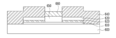
Method of manufacturing transparent transistor with multi-layered structures
PatentInactiveUS20120315729A1
Innovation
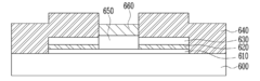
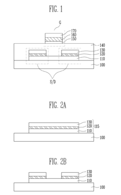
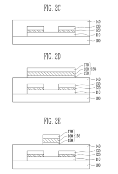
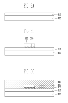
- A stacked structure for transparent transistors is implemented, comprising a substrate with source and drain electrodes having a multi-layered structure of a lower transparent layer, a metal layer, and an upper transparent layer, where the lower and upper transparent layers are formed of the same transparent semiconductor material, and a gate electrode is aligned with the channel, potentially including nitride layers for enhanced refractive index and conductivity.
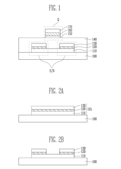
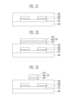
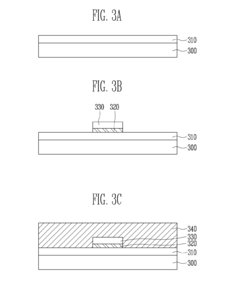
Transparent transistor and method of manufacturing the same
PatentInactiveUS20100155792A1
Innovation
- A stacked structure for transparent transistors is implemented, comprising a substrate with source and drain electrodes having a multi-layered structure of a lower transparent layer, a metal layer, and an upper transparent layer, where the lower and upper transparent layers are formed of the same transparent semiconductor material, and a gate electrode is aligned with the channel, potentially including nitride layers for enhanced refractive index and conductivity.
Manufacturing Scalability Considerations
The scalability of transparent transistor manufacturing represents a critical factor in the widespread adoption of these technologies for sensor applications. Current manufacturing processes for transparent transistors face significant challenges when transitioning from laboratory-scale production to industrial mass production. The primary obstacle lies in maintaining consistent optical transparency and electrical performance across large substrate areas while ensuring cost-effectiveness.
Metal oxide semiconductors, particularly indium gallium zinc oxide (IGZO), have demonstrated promising scalability potential through established techniques such as sputtering and atomic layer deposition. These methods allow for uniform thin film deposition across large areas, making them compatible with existing display manufacturing infrastructure. However, the precise control of oxygen vacancies and metal stoichiometry during large-scale production remains challenging, often resulting in performance variations between production batches.
Roll-to-roll processing emerges as a particularly promising approach for scaling transparent transistor production, especially for flexible sensor applications. This continuous manufacturing technique enables high-throughput production on polymer substrates, though it introduces additional complexities in maintaining film uniformity and adhesion during the mechanical stresses of the rolling process. Recent advancements in tension control systems and in-line quality monitoring have improved yield rates from approximately 60% to over 85% in pilot production lines.
Temperature sensitivity presents another significant manufacturing challenge. Many transparent conducting oxides require specific annealing temperatures to achieve optimal performance, which can limit compatibility with temperature-sensitive substrates like flexible polymers. Low-temperature processing techniques, including solution-based methods and photonic curing, are being developed to address this limitation, though they currently struggle to match the performance of high-temperature processed devices.
Material supply chain considerations also impact manufacturing scalability. The reliance on indium in many transparent transistor designs raises sustainability concerns due to its limited global supply. Alternative material systems using more abundant elements such as zinc tin oxide (ZTO) or aluminum zinc oxide (AZO) are being investigated, though they currently exhibit lower carrier mobility compared to indium-based alternatives.
Integration with existing manufacturing ecosystems represents the final hurdle for scalable production. The ability to incorporate transparent transistor fabrication into established semiconductor or display manufacturing lines would significantly reduce implementation costs. Recent collaborations between research institutions and display manufacturers have demonstrated promising results in this direction, with several pilot lines now capable of producing transparent transistor backplanes at sizes exceeding 15 inches diagonal with defect densities below 0.1 defects per square centimeter.
Integration Challenges with Existing Sensor Systems
The integration of transparent transistors with existing sensor systems presents significant technical challenges that require careful consideration. Current sensor infrastructures are predominantly built around conventional silicon-based electronics, creating compatibility issues when introducing transparent components. The difference in operating parameters, including voltage thresholds, signal processing requirements, and power consumption profiles, necessitates substantial interface engineering to ensure seamless operation between transparent transistors and traditional sensor elements.
Material interface challenges represent another critical barrier to integration. The junction between transparent conductive oxides (TCOs) like indium gallium zinc oxide (IGZO) and conventional materials often creates electrical discontinuities that can degrade signal quality. These heterojunctions frequently exhibit increased resistance and capacitance effects that must be mitigated through specialized interface layers or novel bonding techniques to maintain signal integrity across the entire sensing system.
Manufacturing process compatibility presents additional complications. Transparent transistor fabrication typically involves different deposition techniques, temperature requirements, and chemical processes compared to standard silicon manufacturing. This process mismatch creates difficulties when attempting to integrate transparent components into existing production lines, often requiring either separate manufacturing steps or complete redesign of fabrication workflows to accommodate both technologies.
Signal processing and conditioning requirements differ substantially between transparent and conventional electronics. Transparent transistors generally exhibit lower carrier mobility and different noise characteristics, necessitating specialized signal amplification and filtering circuits. These differences often require redesigned analog front-end systems to properly condition signals from transparent components before they can interface with standard digital processing units.
Environmental stability mismatches further complicate integration efforts. Many transparent semiconductor materials demonstrate different responses to humidity, temperature fluctuations, and UV exposure compared to silicon-based components. These varying degradation mechanisms can lead to differential aging within hybrid systems, potentially causing premature failure at integration points or unpredictable drift in sensor performance over time.
Packaging solutions represent a final significant challenge. Traditional hermetic sealing approaches may obscure the optical properties that make transparent transistors valuable, while alternative packaging methods may not provide adequate protection for sensitive components. This necessitates the development of specialized encapsulation techniques that maintain transparency while ensuring sufficient environmental protection and mechanical stability for practical deployment in real-world sensing applications.
Unlock deeper insights with PatSnap Eureka Quick Research — get a full tech report to explore trends and direct your research. Try now!
Generate Your Research Report Instantly with AI Agent
Supercharge your innovation with PatSnap Eureka AI Agent Platform!