Research on Transparent Transistor Materials Suitable for Harsh Environments
OCT 21, 202510 MIN READ
Generate Your Research Report Instantly with AI Agent
PatSnap Eureka helps you evaluate technical feasibility & market potential.
Transparent Transistor Evolution and Research Objectives
Transparent transistors have evolved significantly since their inception in the early 2000s, transitioning from laboratory curiosities to essential components in modern display technologies. The initial development focused primarily on zinc oxide-based materials, which demonstrated reasonable electron mobility but suffered from stability issues. As research progressed, indium gallium zinc oxide (IGZO) emerged as a breakthrough material around 2010, offering superior performance characteristics and enabling the commercial adoption of transparent electronics in consumer displays.
The harsh environment applications represent a new frontier for transparent transistor technology. Traditional transparent conducting oxides (TCOs) face significant challenges when exposed to extreme temperatures, radiation, corrosive chemicals, or mechanical stress. These environmental factors can cause degradation of electrical properties, structural integrity, and optical transparency, severely limiting their practical applications in aerospace, automotive, deep-sea exploration, and nuclear facilities.
Recent research has shifted toward developing robust transparent transistor materials that maintain functionality under extreme conditions. Gallium oxide (Ga2O3) has shown promising temperature stability up to 600°C, while aluminum nitride (AlN) demonstrates exceptional resistance to radiation damage. Diamond-based transparent semiconductors represent another emerging direction, offering unparalleled hardness and thermal conductivity alongside potential transparency when properly engineered.
The primary technical objectives of current research include enhancing the temperature stability of transparent transistors beyond 700°C, improving radiation hardness to withstand exposure exceeding 1 MGy, and developing materials with chemical resistance to highly corrosive environments. Additionally, researchers aim to maintain optical transparency above 80% in the visible spectrum while achieving electron mobility exceeding 10 cm²/Vs under harsh conditions.
From a manufacturing perspective, research goals include developing scalable deposition techniques compatible with temperature-sensitive substrates and establishing reliable encapsulation methods to protect devices from environmental degradation. The integration of these materials with flexible substrates represents another significant challenge, particularly for applications requiring both mechanical flexibility and environmental resilience.
The long-term vision for this technology encompasses self-healing transparent electronics that can automatically recover from environmental damage, as well as adaptive systems that modify their electrical properties in response to changing environmental conditions. These advanced capabilities would enable unprecedented applications in extreme environments where conventional electronics fail, opening new possibilities for sensing, communication, and control systems in previously inaccessible locations.
Market Analysis for Harsh Environment Electronics
The harsh environment electronics market is experiencing robust growth, driven by increasing demand across multiple sectors including aerospace, defense, automotive, industrial automation, and energy exploration. These environments subject electronic components to extreme temperatures, radiation, chemical exposure, and mechanical stress, necessitating specialized materials and designs. The global market for harsh environment electronics was valued at approximately 2.1 billion USD in 2022 and is projected to reach 3.8 billion USD by 2028, representing a compound annual growth rate of 10.3%.
Transparent transistor materials for harsh environments represent a particularly promising segment within this market. The need for displays and sensors that can withstand extreme conditions while maintaining optical transparency has created significant commercial opportunities. Industries such as military avionics, deep-sea exploration, space technology, and high-temperature manufacturing processes are primary drivers of this demand.
The automotive sector constitutes a substantial portion of the market, with requirements for dashboard displays and sensors that can withstand temperature extremes and vibration. The increasing electrification of vehicles and advancement of autonomous driving technologies has further accelerated demand for harsh-environment capable transparent electronics.
The aerospace and defense sectors collectively account for approximately 35% of the market share, where transparent displays and control systems must function reliably in conditions ranging from the vacuum of space to hypersonic flight environments. These applications typically command premium pricing due to stringent performance and reliability requirements.
Geographically, North America leads the market with approximately 40% share, followed by Europe and Asia-Pacific. However, the Asia-Pacific region is experiencing the fastest growth rate, driven by increasing industrial automation and defense modernization programs in countries like China, Japan, and South Korea.
The energy sector, particularly oil and gas exploration, represents another significant market segment. Downhole tools and monitoring systems operating in environments exceeding 200°C with high pressure and corrosive conditions require specialized transparent electronic components that can maintain functionality and optical clarity.
Market analysts identify several key trends shaping future demand: miniaturization of components, integration of multiple functionalities into single devices, and increasing requirements for energy efficiency. Additionally, the growing Internet of Things (IoT) ecosystem is creating demand for sensor networks that can operate in previously inaccessible environments, further expanding market opportunities for transparent transistor materials designed for harsh conditions.
Current Limitations of Transparent Transistor Materials
Despite significant advancements in transparent transistor technology, current materials face substantial limitations when deployed in harsh environments. Conventional transparent conducting oxides (TCOs) such as indium tin oxide (ITO) and zinc oxide (ZnO) exhibit performance degradation when exposed to extreme temperatures, with most materials showing significant conductivity loss above 200°C or below -40°C. This thermal instability restricts their application in aerospace, automotive, and industrial settings where temperature fluctuations are common.
Chemical stability presents another critical challenge, as many transparent transistor materials demonstrate poor resistance to corrosive environments. Exposure to acids, bases, or oxidizing agents can lead to rapid deterioration of electrical properties and physical integrity. For instance, ZnO-based transistors show marked degradation when exposed to humidity above 70% relative humidity, limiting their deployment in marine or tropical environments.
Mechanical durability remains problematic, with most transparent materials exhibiting brittleness under mechanical stress. Current materials typically fail after 1,000-10,000 bending cycles, making them unsuitable for flexible electronics applications in harsh conditions. This limitation is particularly evident in amorphous oxide semiconductors that crack under minimal strain, leading to catastrophic device failure.
Radiation resistance represents a significant barrier for applications in space, nuclear facilities, or medical imaging environments. Conventional transparent semiconductors experience performance shifts due to radiation-induced defects, with threshold voltage shifts exceeding 2V after exposure to just 10 kGy of gamma radiation. These radiation effects can permanently alter carrier concentration and mobility, rendering devices inoperable.
Long-term reliability under combined stressors remains largely unaddressed in current material systems. When exposed simultaneously to thermal cycling, mechanical stress, and chemical agents—conditions common in real-world harsh environments—most transparent transistor materials show accelerated degradation with mean time to failure often reduced by 60-80% compared to single-stressor testing.
Manufacturing scalability presents additional challenges, as many laboratory-demonstrated materials with improved harsh environment performance rely on expensive deposition techniques or rare elements. The trade-off between transparency, electrical performance, and environmental stability often results in compromised designs that fail to meet industrial requirements for harsh environment applications.
Interface stability between different material layers in transparent transistor structures deteriorates rapidly in harsh conditions, with delamination and interfacial reactions becoming prevalent. This leads to increased contact resistance and eventual device failure, particularly at the critical semiconductor-dielectric interface where carrier transport occurs.
Current Material Solutions for Harsh Environment Applications
01 Metal oxide semiconductor materials for transparent transistors
Metal oxide semiconductors such as indium gallium zinc oxide (IGZO), zinc oxide (ZnO), and tin oxide (SnO2) are widely used in transparent transistor applications due to their high optical transparency and electrical performance. These materials can achieve transparency levels exceeding 80% in the visible spectrum while maintaining good electron mobility. The amorphous structure of these oxides contributes to uniform performance across large areas, making them suitable for display applications where both transparency and durability are required.- Metal oxide semiconductor materials for transparent transistors: Metal oxide semiconductors such as indium gallium zinc oxide (IGZO), zinc oxide (ZnO), and tin oxide (SnO2) are widely used in transparent transistor applications due to their high optical transparency and electrical performance. These materials can achieve transparency levels exceeding 80% in the visible spectrum while maintaining good electron mobility. The amorphous structure of these oxides allows for uniform performance across large areas and enables fabrication on flexible substrates, enhancing durability and expanding application possibilities.
- Carbon-based transparent conductive materials: Carbon-based materials such as graphene, carbon nanotubes (CNTs), and reduced graphene oxide offer excellent transparency and mechanical flexibility for transistor applications. These materials combine high optical transparency with superior mechanical strength and durability, making them suitable for flexible and stretchable electronics. Their unique structure allows for maintaining electrical conductivity even under mechanical stress, and they can be processed at lower temperatures compared to traditional semiconductor materials, enabling compatibility with a wider range of substrates.
- Protective coating technologies for enhanced durability: Various protective coating technologies have been developed to enhance the durability of transparent transistors. These include atomic layer deposition (ALD) of aluminum oxide or hafnium oxide layers, which provide excellent barrier properties against moisture and oxygen. Specialized polymer encapsulation techniques using materials like parylene or polyimide offer additional mechanical protection while maintaining transparency. These protective layers significantly extend device lifetime by preventing degradation from environmental factors while preserving the optical and electrical properties of the underlying transistor materials.
- Composite and hybrid transparent materials: Composite and hybrid materials combining inorganic semiconductors with organic components offer enhanced transparency and durability characteristics. These materials leverage the high transparency of organic polymers with the electrical stability of inorganic semiconductors. Nanocomposites incorporating metal oxide nanoparticles in polymer matrices provide tunable optical and electrical properties while improving mechanical flexibility. The synergistic effects of these hybrid structures result in transistors with improved resistance to mechanical stress and environmental degradation while maintaining high transparency levels.
- Processing techniques for optimizing transparency and durability: Advanced processing techniques play a crucial role in optimizing both transparency and durability of transistor materials. Low-temperature deposition methods such as solution processing and sputtering enable fabrication on temperature-sensitive substrates while maintaining material quality. Post-deposition treatments including annealing in controlled atmospheres and surface passivation techniques can significantly improve material stability and optical properties. Specialized patterning methods that minimize edge defects and stress concentration points further enhance the mechanical durability of transparent transistor structures while preserving their electrical performance.
02 Carbon-based transparent conductive materials
Carbon-based materials such as graphene, carbon nanotubes, and conductive polymers offer alternatives to traditional transparent conductive oxides. These materials provide excellent flexibility and mechanical durability while maintaining high transparency. Graphene, a single layer of carbon atoms, exhibits exceptional optical transparency (>97%) with good electrical conductivity. Carbon nanotubes can be formulated into networks that balance transparency and conductivity requirements for flexible transparent transistor applications, while also providing superior resistance to mechanical stress and bending.Expand Specific Solutions03 Protective coating technologies for enhanced durability
Various protective coating technologies have been developed to enhance the durability of transparent transistor materials. These include atomic layer deposition of alumina or other metal oxides to create barrier layers against moisture and oxygen penetration. Hybrid organic-inorganic coatings provide both mechanical protection and chemical stability. Self-healing polymer coatings can repair minor damage automatically, extending device lifetime. These protective layers are designed to maintain the optical transparency of the underlying transistor materials while significantly improving their resistance to environmental factors and physical damage.Expand Specific Solutions04 Nanocomposite materials for transparency-durability balance
Nanocomposite materials combine different components at the nanoscale to achieve an optimal balance between transparency and durability. These materials typically incorporate nanoparticles or nanostructures within a transparent matrix to enhance mechanical properties without significantly compromising optical transparency. For example, silica nanoparticles dispersed in polymer matrices can improve scratch resistance and hardness while maintaining high light transmission. Other approaches include embedding conductive nanowires in transparent polymers to create flexible, durable transparent electrodes for transistor applications.Expand Specific Solutions05 Processing techniques for optimizing transparency and durability
Advanced processing techniques play a crucial role in optimizing both the transparency and durability of transistor materials. Low-temperature deposition methods such as solution processing and room-temperature sputtering allow for the fabrication of transparent transistors on flexible substrates without thermal damage. Post-deposition treatments including annealing, plasma treatment, and surface modification can significantly improve the crystallinity, interface quality, and environmental stability of transparent conductive materials. These processing approaches enable the production of transparent transistors with enhanced optical clarity and resistance to degradation under operating conditions.Expand Specific Solutions
Industry Leaders in Transparent Electronics
The transparent transistor materials market for harsh environments is currently in an early growth phase, characterized by increasing R&D investments and emerging commercial applications. The global market size is projected to expand significantly as industries like aerospace, defense, and automotive seek robust electronics for extreme conditions. Technologically, the field shows moderate maturity with several key players driving innovation. Wolfspeed leads in wide bandgap semiconductors (SiC and GaN), while Semiconductor Energy Laboratory specializes in IGZO technology. Universities like Tsinghua, Tokyo Institute of Technology, and Northwestern contribute fundamental research. Electronics giants including Sharp, NEC, and Canon are developing practical applications, while specialty materials companies like DuPont and Resonac provide essential components. The ecosystem reflects a balance between academic research and industrial commercialization efforts.
Purdue Research Foundation
Technical Solution: Purdue Research Foundation has developed innovative transparent transistor materials based on atomic layer deposition (ALD) of zinc oxide (ZnO) and related compounds specifically engineered for harsh environment applications. Their approach focuses on creating highly uniform, defect-free thin films with precisely controlled interfaces that maintain electrical performance under extreme conditions. Purdue researchers have pioneered specialized annealing techniques that enhance crystallinity while preserving transparency, resulting in devices with mobility values exceeding 20 cm²/Vs even after exposure to temperatures above 250°C. Their transparent transistors incorporate unique dielectric engineering with high-k materials like HfO2 and Al2O3 in optimized multilayer structures that provide exceptional gate stability under thermal and electrical stress. Additionally, Purdue has developed novel surface passivation methods using self-assembled monolayers that significantly reduce interface trap states, enhancing stability against moisture, radiation, and chemical exposure while maintaining transparency above 85% across the visible spectrum.
Strengths: Industry-leading mobility values maintained under harsh conditions; excellent interface engineering minimizes performance degradation; innovative passivation techniques enhance environmental stability; compatible with flexible substrate integration. Weaknesses: Complex fabrication processes may challenge mass production; some specialized materials increase production costs; requires careful optimization for specific harsh environment applications.
Wolfspeed, Inc.
Technical Solution: Wolfspeed has developed advanced wide-bandgap semiconductor materials, primarily focusing on silicon carbide (SiC) and gallium nitride (GaN) technologies for transparent transistor applications in harsh environments. Their approach leverages the inherent temperature stability and radiation resistance of these materials while engineering novel device architectures to enhance transparency. Wolfspeed's SiC-based transparent transistors utilize ultra-thin film deposition techniques that maintain optical transparency while preserving the material's exceptional thermal conductivity (>3.5 W/cm·K) and breakdown field strength (>2.5 MV/cm). For extreme environment applications, they've pioneered specialized surface passivation techniques and edge termination structures that prevent performance degradation under high-temperature, high-radiation, or chemically corrosive conditions. Their transistors demonstrate stable operation at temperatures exceeding 300°C with minimal leakage current increases, making them ideal for deep-well drilling, aerospace, and industrial furnace control applications.
Strengths: Superior high-temperature performance (stable operation >300°C); excellent power handling capabilities; inherent radiation hardness; long-term reliability in corrosive environments. Weaknesses: Higher manufacturing complexity and cost; lower transparency levels compared to oxide semiconductor alternatives; requires specialized packaging solutions for harsh environment deployment.
Key Patents in Transparent Transistor Material Science
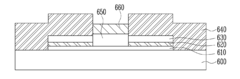
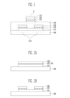
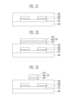
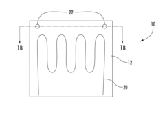
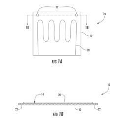
Method of manufacturing transparent transistor with multi-layered structures
PatentInactiveUS20120315729A1
Innovation
- A stacked structure for transparent transistors is implemented, comprising a substrate with source and drain electrodes having a multi-layered structure of a lower transparent layer, a metal layer, and an upper transparent layer, where the lower and upper transparent layers are formed of the same transparent semiconductor material, and a gate electrode is aligned with the channel, potentially including nitride layers for enhanced refractive index and conductivity.
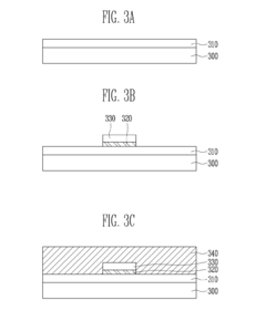
Silica content substrate such as for use harsh environment circuits and high frequency antennas
PatentActiveUS10015879B2
Innovation
- A high-silica content substrate with a low coefficient of thermal expansion and unique surface features, such as raised and recessed features, is developed, allowing for enhanced bonding and metallization, along with high purity and low dielectric properties, facilitating the creation of thin, flexible, and robust circuits suitable for high-frequency applications.
Material Stability and Degradation Mechanisms
Transparent transistors operating in harsh environments face significant material stability challenges that must be thoroughly understood to develop reliable solutions. The primary degradation mechanisms affecting these materials can be categorized into thermal, chemical, radiation, and mechanical stresses, each contributing to performance deterioration through distinct pathways.
Thermal degradation represents a critical concern, particularly in high-temperature environments exceeding 300°C. Metal oxide semiconductors such as IGZO and ZnO exhibit phase transformations and crystallization processes that alter their electrical properties. Studies have shown that amorphous IGZO begins to crystallize at approximately 500°C, resulting in grain boundary formation that significantly reduces carrier mobility and increases threshold voltage instability.
Chemical degradation occurs through interaction with environmental contaminants, particularly moisture and reactive gases. Water molecules can penetrate the material structure, creating hydroxyl groups that act as electron traps at the semiconductor-dielectric interface. This phenomenon is especially pronounced in oxide semiconductors, where oxygen vacancies serve as primary conduction pathways. Hydrogen diffusion from ambient moisture has been documented to cause persistent photoconductivity effects in ZnO-based transistors, leading to threshold voltage shifts exceeding 2V after prolonged exposure.
Radiation-induced degradation presents unique challenges in aerospace and nuclear applications. High-energy particles create defect states within the bandgap, altering carrier concentration and mobility. Interestingly, certain transparent oxide semiconductors demonstrate superior radiation hardness compared to silicon-based alternatives. Recent research indicates that Ga₂O₃-based transistors maintain functionality after exposure to gamma radiation doses up to 1 MGy, though with degraded on/off ratios.
Mechanical stress effects manifest through lattice deformation and microcrack formation, particularly relevant for flexible transparent electronics. Repeated bending cycles induce strain at material interfaces, leading to delamination and performance degradation. Studies on flexible IGZO transistors reveal that tensile strain exceeding 2% can increase off-state current by several orders of magnitude due to defect generation at the semiconductor-dielectric interface.
The combined effects of these degradation mechanisms often exhibit synergistic behavior, where simultaneous exposure to multiple stressors accelerates material failure beyond the sum of individual effects. For instance, elevated temperatures significantly enhance moisture-induced degradation rates, with reaction kinetics approximately doubling with every 10°C increase. Understanding these complex interactions requires comprehensive accelerated aging studies that simulate real-world operating conditions while monitoring electrical parameter shifts and material structure changes.
Environmental Impact and Sustainability Considerations
The development and deployment of transparent transistors for harsh environments necessitates careful consideration of environmental impacts throughout their lifecycle. Manufacturing processes for transparent oxide semiconductors often involve energy-intensive deposition techniques such as sputtering, chemical vapor deposition, and atomic layer deposition, which contribute significantly to carbon emissions. Additionally, these processes typically require rare earth elements and metals like indium, gallium, and zinc, whose extraction causes substantial environmental degradation including habitat destruction, water pollution, and soil contamination.
Material selection presents both challenges and opportunities for sustainability. While traditional transparent conducting oxides like indium tin oxide (ITO) rely on scarce resources, emerging alternatives such as graphene, carbon nanotubes, and conductive polymers offer potentially lower environmental footprints. These materials can be synthesized from more abundant resources and may require less energy-intensive processing methods, though scale-up challenges remain significant barriers to widespread adoption.
Durability in harsh environments directly impacts sustainability through extended product lifecycles. Transparent transistors designed to withstand extreme temperatures, radiation, or chemical exposure reduce replacement frequency and associated waste generation. This longevity is particularly valuable in remote sensing applications, aerospace systems, and industrial monitoring equipment where maintenance access is limited and replacement costs are substantial.
End-of-life considerations reveal significant recycling challenges for transparent electronics. The complex integration of multiple materials in thin-film structures complicates material recovery processes. Current recycling technologies struggle to efficiently separate and recover valuable components from transparent transistor assemblies, resulting in substantial material loss. Research into design-for-disassembly approaches and advanced recycling technologies specifically tailored for transparent electronics represents a critical area for future development.
Water consumption during manufacturing presents another environmental concern, particularly for facilities located in water-stressed regions. Fabrication processes typically require ultrapure water for cleaning and processing steps, with significant volumes consumed per unit produced. Implementation of closed-loop water recycling systems and process optimization can substantially reduce this impact, though such systems require additional capital investment.
Regulatory frameworks increasingly influence material selection and manufacturing processes for transparent electronics. Restrictions on hazardous substances like lead, mercury, and certain flame retardants drive innovation toward more environmentally benign alternatives. Future-proofing transparent transistor technologies requires anticipating regulatory trends and proactively developing compliant solutions that maintain performance requirements for harsh environment applications.
Unlock deeper insights with PatSnap Eureka Quick Research — get a full tech report to explore trends and direct your research. Try now!
Generate Your Research Report Instantly with AI Agent
Supercharge your innovation with PatSnap Eureka AI Agent Platform!