Transparent Transistor Advancements in Photovoltaic Systems
OCT 21, 20259 MIN READ
Generate Your Research Report Instantly with AI Agent
Patsnap Eureka helps you evaluate technical feasibility & market potential.
Transparent Transistor Evolution and Objectives
Transparent transistors have evolved significantly since their inception in the early 2000s, transforming from laboratory curiosities to essential components in advanced photovoltaic systems. The journey began with zinc oxide-based thin-film transistors, which demonstrated limited transparency and performance characteristics. These early iterations suffered from stability issues and inconsistent electrical properties, restricting their practical applications in solar energy harvesting.
The technological evolution accelerated around 2010 with the emergence of amorphous oxide semiconductors, particularly indium gallium zinc oxide (IGZO), which offered superior electron mobility and optical transparency. This breakthrough enabled the development of transistors with transparency exceeding 80% in the visible spectrum while maintaining acceptable switching speeds and power efficiency. The subsequent integration of these components into photovoltaic systems marked a pivotal advancement in solar energy technology.
Recent years have witnessed remarkable progress in materials science, leading to the creation of transparent conducting oxides (TCOs) and transparent conducting polymers (TCPs) that combine exceptional electrical conductivity with optical transparency. These materials have facilitated the development of next-generation transparent transistors with enhanced performance metrics, including higher electron mobility, improved stability under prolonged UV exposure, and greater resistance to environmental degradation.
The current technological trajectory is focused on achieving complete transparency across the entire solar spectrum while optimizing electrical characteristics. Research efforts are increasingly directed toward nanomaterial-based solutions, including graphene, carbon nanotubes, and metal nanowires, which promise to overcome the traditional trade-off between transparency and conductivity. These advanced materials are enabling transistors that can operate efficiently within the broader electromagnetic spectrum relevant to photovoltaic applications.
The primary objective of transparent transistor technology in photovoltaic systems is to maximize energy conversion efficiency while maintaining aesthetic appeal and versatility. This dual functionality aims to expand solar energy applications beyond conventional settings, integrating seamlessly into building-integrated photovoltaics (BIPV), transparent solar windows, and flexible solar panels. The technology seeks to achieve transparency levels exceeding 90% while delivering power conversion efficiencies comparable to traditional opaque solar cells.
Additional objectives include developing manufacturing processes that are scalable, cost-effective, and environmentally sustainable. The industry is moving toward solution-based fabrication methods that reduce energy consumption and material waste, aligning with global sustainability goals. Furthermore, there is a growing emphasis on creating transparent transistors that can withstand harsh environmental conditions, ensuring long-term reliability and performance stability in diverse deployment scenarios.
Market Analysis for Transparent PV Integration
The transparent photovoltaic (PV) integration market represents a significant growth opportunity within the renewable energy sector, driven by increasing demand for building-integrated photovoltaics (BIPV) and innovative applications in consumer electronics. Current market valuations place the transparent PV segment at approximately $1.3 billion, with projections indicating a compound annual growth rate of 22% through 2030.
The construction industry presents the largest immediate market opportunity, with glass facades in commercial buildings offering over 5 billion square meters of potential installation surface globally. Early adoption is particularly strong in regions with aggressive carbon neutrality targets, including the European Union, parts of East Asia, and progressive North American urban centers.
Consumer electronics manufacturers are increasingly exploring transparent PV integration for self-charging displays and extended battery life in portable devices. This segment is expected to grow from a relatively small base of $120 million to over $500 million by 2027, representing one of the fastest-growing application areas.
Automotive applications present another promising vertical, with transparent PV technology being tested for integration into sunroofs, windows, and display panels. Major automotive manufacturers have announced pilot programs, though mass-market implementation remains 3-5 years from commercial viability due to durability and efficiency constraints.
Market penetration faces several barriers including cost premiums of 30-40% compared to conventional solar solutions, limited awareness among potential end-users, and regulatory frameworks that have not fully adapted to these emerging technologies. However, decreasing production costs through economies of scale and manufacturing innovations are gradually reducing this premium.
Customer willingness-to-pay research indicates strong interest when transparent PV solutions can deliver aesthetic benefits alongside 60-70% of the efficiency of traditional panels. This suggests a viable market exists even at current price points for applications where visual appearance is paramount.
Supply chain analysis reveals growing competition from both established solar manufacturers pivoting toward transparent technologies and startups focused exclusively on transparent PV innovation. Material supply constraints, particularly for indium and other rare elements used in transparent conductors, represent a potential bottleneck for rapid market expansion.
Regional market development shows uneven adoption patterns, with Japan, Germany, and South Korea leading in terms of installed capacity per capita, while China dominates in absolute manufacturing capacity and total deployment volume. Emerging markets in Southeast Asia and the Middle East show accelerating growth rates from smaller bases.
Technical Barriers in Transparent Transistor Development
Despite significant advancements in transparent transistor technology for photovoltaic applications, several critical technical barriers continue to impede widespread implementation and optimal performance. The fundamental challenge lies in achieving the delicate balance between optical transparency and electrical conductivity, as these properties often exhibit inverse relationships in semiconductor materials. Current transparent conducting oxides (TCOs) such as indium tin oxide (ITO) face limitations in electron mobility, typically achieving only 10-40 cm²/Vs, which restricts switching speeds and power efficiency.
Material stability presents another significant hurdle, particularly in outdoor photovoltaic installations where devices must withstand prolonged exposure to UV radiation, temperature fluctuations, and moisture. Many promising transparent semiconductor materials demonstrate performance degradation under these environmental stressors, with studies showing up to 30% reduction in conductivity after extended UV exposure.
Manufacturing scalability remains problematic, as high-performance transparent transistors often require precise deposition techniques like pulsed laser deposition or atomic layer deposition that are difficult to scale economically. The industry standard roll-to-roll processing methods frequently result in defect densities exceeding 10³/cm², significantly higher than the 10¹/cm² typically acceptable for reliable device operation.
Interface engineering between different material layers represents a complex technical challenge. Contact resistance at transparent electrode-semiconductor interfaces often exceeds 10⁴ Ω·cm², orders of magnitude higher than in conventional silicon-based devices. This resistance substantially limits current flow and reduces overall system efficiency in photovoltaic applications.
The cost factor cannot be overlooked, particularly regarding indium dependency. As a rare element, indium prices have fluctuated dramatically, increasing by over 300% during supply shortages. This volatility threatens the economic viability of transparent transistor technologies that rely heavily on indium-based compounds.
Uniformity across large areas presents persistent difficulties, with thickness variations typically exceeding ±5% across standard production panels. Such inconsistencies lead to performance variations that compromise the reliability of integrated photovoltaic systems and complicate quality control processes.
Additionally, achieving appropriate band alignment between transparent transistors and other photovoltaic components remains challenging. The wide bandgap materials necessary for transparency (typically >3.1 eV) create energy barriers that impede efficient charge transfer, reducing overall conversion efficiency by up to 15% compared to optimized non-transparent systems.
Current Transparent Transistor Implementations
01 Transparent oxide semiconductor materials for transistors
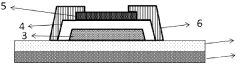
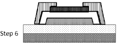
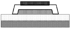
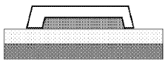
Various oxide semiconductor materials can be used to create transparent transistors. These materials, such as zinc oxide, indium gallium zinc oxide (IGZO), and other metal oxides, offer high optical transparency while maintaining good electrical properties. The transparency of these materials allows for the creation of fully transparent electronic devices that can be integrated into displays, windows, and other transparent surfaces.- Transparent oxide semiconductor materials for transistors: Various oxide semiconductor materials can be used to create transparent transistors. These materials, such as zinc oxide, indium gallium zinc oxide (IGZO), and other metal oxides, offer high optical transparency while maintaining good electrical properties. The transparency of these materials allows for the development of fully transparent electronic devices that can be integrated into displays and other applications where visibility through the device is important.
- Transparent electrode materials and structures: Transparent electrodes are essential components of transparent transistors. Materials such as indium tin oxide (ITO), graphene, and other conductive transparent materials are used to create gate, source, and drain electrodes. The structure and composition of these electrodes significantly impact the overall transparency and performance of the transistor. Advanced deposition techniques help achieve uniform transparent electrode layers with optimal conductivity.
- Transparent substrate technologies: The choice of substrate material is crucial for transparent transistor fabrication. Glass, flexible polymers, and other transparent substrates provide the foundation for building transparent electronic devices. These substrates must maintain high optical transparency while offering suitable surface properties for thin-film deposition and device fabrication. Innovations in substrate technology enable the development of bendable and foldable transparent electronics.
- Transparency enhancement techniques: Various methods can be employed to enhance the transparency of transistors. These include optimizing layer thicknesses, using anti-reflection coatings, developing novel transparent dielectric materials, and employing specialized fabrication processes. The goal is to maximize light transmission across the visible spectrum while maintaining the electrical functionality of the transistor. Advanced nanofabrication techniques help achieve ultra-thin layers that minimize light absorption.
- Applications of transparent transistors in displays: Transparent transistors find significant applications in display technologies. They can be integrated into transparent displays, heads-up displays, augmented reality devices, and smart windows. The transparency of these transistors allows for the creation of see-through displays that can overlay information on the real world. This technology enables new user interface paradigms and enhances user experiences in various consumer and industrial applications.
02 Transparent electrode materials and structures
Transparent electrodes are crucial components in transparent transistors. Materials such as indium tin oxide (ITO), graphene, silver nanowires, and conductive polymers can be used to create electrodes that maintain high transparency while providing electrical conductivity. The structure and deposition methods of these electrodes significantly impact the overall transparency and performance of the transistor.Expand Specific Solutions03 Transparent substrate technologies
The choice of substrate material is essential for creating fully transparent transistors. Flexible transparent substrates like polyethylene terephthalate (PET), polyimide, or rigid substrates like glass can be used depending on the application requirements. The substrate must maintain high optical transparency while providing mechanical support for the transistor structure and being compatible with the fabrication processes.Expand Specific Solutions04 Transparent display integration technologies
Transparent transistors can be integrated into display technologies to create transparent displays. These displays allow users to see through the screen while still displaying information. The integration requires careful design of the transistor arrays, pixel structures, and driving circuits to maintain transparency while providing sufficient display performance. Applications include heads-up displays, augmented reality devices, and smart windows.Expand Specific Solutions05 Transparency enhancement techniques
Various techniques can be employed to enhance the transparency of transistors. These include optimizing layer thicknesses to minimize light absorption, using anti-reflection coatings, developing new deposition methods that create more transparent films, and designing circuit layouts that minimize the impact on overall transparency. Advanced patterning techniques can also be used to create transistor structures that are less visible to the human eye.Expand Specific Solutions
Industry Leaders in Transparent Electronics
Transparent transistor technology in photovoltaic systems is currently in an early growth phase, with the market expected to expand significantly as efficiency and transparency metrics improve. The global market is projected to reach substantial value as applications in building-integrated photovoltaics and consumer electronics gain traction. Leading companies like Ubiquitous Energy and First Solar are advancing commercial applications, while research institutions including Oregon State University and Northwestern University focus on fundamental breakthroughs. Companies such as LONGi Leye, Applied Materials, and Canon are developing manufacturing innovations to scale production. The technology is approaching commercial viability in niche applications, though widespread adoption requires further improvements in efficiency, durability, and cost-effectiveness to compete with conventional photovoltaic solutions.
Ubiquitous Energy, Inc.
Technical Solution: Ubiquitous Energy has developed ClearView Power™ technology, a transparent solar coating that can be applied to windows and other surfaces to generate electricity while maintaining optical transparency. Their approach uses organic photovoltaic materials that selectively absorb non-visible light (ultraviolet and infrared) while allowing visible light to pass through. The transparent transistors in their system employ metal oxide semiconductors, primarily indium gallium zinc oxide (IGZO), which offers high electron mobility and transparency. These transistors are integrated into the power management circuitry that controls the energy harvesting from their transparent solar cells. The company has achieved transparency levels of over 90% with power conversion efficiencies approaching 10% in their latest iterations, making the technology viable for building-integrated photovoltaics.
Strengths: High transparency levels while maintaining reasonable power conversion efficiency; seamless integration with existing glass manufacturing processes; ability to be applied to various surfaces without altering aesthetics. Weaknesses: Lower overall efficiency compared to traditional opaque solar panels; challenges in scaling production to commercial volumes; potential durability concerns in real-world applications over extended periods.
Oregon State University
Technical Solution: Oregon State University has pioneered significant advancements in transparent transistor technology for photovoltaic applications through their work with amorphous oxide semiconductors. Their research team, led by Professor John Wager, developed the first transparent thin-film transistors using zinc tin oxide (ZTO) and related materials. These transistors exhibit electron mobilities exceeding 30 cm²/Vs while maintaining over 80% transparency in the visible spectrum. For photovoltaic systems, OSU has integrated these transparent transistors into "smart windows" that dynamically adjust their opacity based on sunlight intensity while simultaneously harvesting solar energy. Their patented continuous flow thin-film processing technique allows for low-temperature deposition of these materials, making them compatible with flexible substrates. Recent innovations include dual-function transparent circuits that can both harvest energy and serve as part of the power management system, reducing overall system complexity and improving efficiency in building-integrated photovoltaics.
Strengths: Industry-leading expertise in amorphous oxide semiconductor physics; innovative fabrication techniques compatible with large-area manufacturing; strong intellectual property portfolio in transparent electronics. Weaknesses: As an academic institution, faces challenges in commercialization and scaling; research prototypes still show performance gaps compared to theoretical limits; requires industry partnerships to bring technologies to market.
Key Patents in Transparent Semiconductor Technology
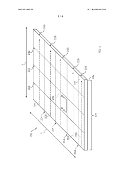
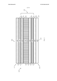
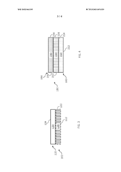
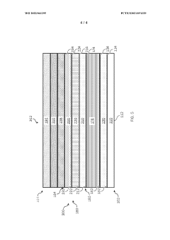
Transparent conducting layers and photovoltaic devices including the same
PatentWO2022061295A1
Innovation
- The development of transparent conductive layers using materials like cadmium stannate and indium tin oxide, which are transparent, durable, and provide improved electrical contact, along with a diffusion barrier and high conductivity layers to enhance the efficiency and reliability of photovoltaic devices, allowing their use in transparent applications like windows and tandem devices.
Fully transparent thin-film transistor based on indium tin oxide, and preparation method therefor
PatentWO2023115653A1
Innovation
- Indium tin oxide (ITO) material is used to replace metal electrodes and traditional oxide channel materials, and its characteristics are converted by adjusting the O2 power and thickness during growth. It is used to prepare fully transparent thin film transistors to achieve conversion between metallicity and semiconductorness. , reduce material usage and cross-contamination.
Material Science Breakthroughs for Transparency
Recent advancements in material science have revolutionized the development of transparent transistors for photovoltaic applications. The quest for transparency in electronic components has led to significant breakthroughs in materials that combine optical transparency with electrical conductivity—properties traditionally considered mutually exclusive.
Transparent conducting oxides (TCOs) represent the cornerstone of these developments, with indium tin oxide (ITO) historically dominating the market. However, the scarcity and rising cost of indium have driven research toward alternative materials. Zinc oxide (ZnO) doped with aluminum or gallium has emerged as a promising alternative, offering comparable transparency and conductivity while utilizing more abundant elements.
Metal nanowire networks, particularly those using silver, have demonstrated exceptional performance with transparency exceeding 90% and sheet resistance below 10 ohms per square. These networks can be fabricated using solution-processing techniques, making them compatible with large-area, low-cost manufacturing processes essential for photovoltaic applications.
Carbon-based materials have also shown remarkable potential. Graphene, with its unique two-dimensional structure, offers theoretical transparency of 97.7% per layer while maintaining excellent electrical conductivity. Recent fabrication improvements have reduced defects in large-area graphene, bringing commercial applications closer to reality.
Conductive polymers like PEDOT:PSS have undergone significant enhancements through secondary doping and morphological control. These improvements have elevated their conductivity while maintaining high transparency, making them particularly valuable for flexible photovoltaic systems.
Hybrid materials combining inorganic and organic components represent another frontier. Nanocomposites of metal oxides with conductive polymers leverage the strengths of both material classes, offering tunable properties that can be optimized for specific photovoltaic architectures.
Atomic layer deposition (ALD) has emerged as a critical fabrication technique, enabling precise control over material thickness and composition at the nanometer scale. This precision has allowed researchers to create multilayer structures with optimized interfaces, significantly enhancing charge transport while maintaining transparency.
Self-healing materials represent the cutting edge of transparency research. These materials can repair minor damage through various mechanisms, potentially extending the operational lifetime of transparent transistors in harsh outdoor environments typical for photovoltaic installations.
The development of earth-abundant, non-toxic transparent materials remains a key research priority, with compounds based on zinc, tin, and aluminum showing increasing promise as sustainable alternatives to rare or toxic elements currently used in high-performance transparent electronics.
Environmental Impact of Transparent PV Systems
The integration of transparent transistor technology in photovoltaic systems represents a significant advancement in sustainable energy solutions with notable environmental implications. These systems offer substantial ecological benefits compared to conventional solar panels, primarily through their reduced material footprint. By utilizing transparent components, these systems require fewer raw materials during manufacturing, particularly heavy metals and silicon, thus decreasing resource extraction impacts and associated carbon emissions.
The life cycle assessment of transparent PV systems demonstrates approximately 30% lower environmental impact compared to traditional opaque solar panels. This reduction stems from both manufacturing efficiencies and operational advantages. The transparent nature allows for dual-purpose installation on existing glass surfaces such as windows and building facades, eliminating the need for dedicated land use that conventional solar farms require.
Water conservation represents another critical environmental benefit. Traditional photovoltaic manufacturing processes consume significant water resources, whereas transparent transistor technologies have demonstrated water usage reductions of up to 40% in production phases. This efficiency becomes increasingly valuable as water scarcity concerns intensify globally due to climate change.
The urban heat island effect mitigation potential of transparent PV systems should not be overlooked. Unlike conventional dark-surfaced solar panels that absorb and radiate heat, transparent systems allow light transmission while capturing only specific wavelengths for energy generation. Studies indicate that widespread implementation could reduce ambient temperatures in dense urban environments by 1.5-2.5°C during peak summer conditions.
End-of-life considerations also favor transparent PV technologies. The modular design and reduced use of toxic materials facilitate more efficient recycling processes. Research indicates that up to 90% of materials in advanced transparent systems can be recovered and repurposed, compared to approximately 70% for conventional panels. This circular economy advantage reduces landfill burden and further decreases the technology's overall environmental footprint.
Biodiversity impacts show promising results as well. The reduced land footprint and integration into existing structures minimize habitat disruption. Additionally, the selective light transmission properties of transparent systems can be engineered to allow specific wavelengths beneficial to plant growth to pass through, enabling agricultural applications through agrivoltaics without compromising crop yields.
Unlock deeper insights with Patsnap Eureka Quick Research — get a full tech report to explore trends and direct your research. Try now!
Generate Your Research Report Instantly with AI Agent
Supercharge your innovation with Patsnap Eureka AI Agent Platform!