Transparent Transistors: Patent Landscape and Emerging Technologies
OCT 21, 202510 MIN READ
Generate Your Research Report Instantly with AI Agent
Patsnap Eureka helps you evaluate technical feasibility & market potential.
Transparent Transistor Evolution and Research Objectives
Transparent transistors have evolved significantly since their inception in the early 2000s, marking a revolutionary advancement in display technology and flexible electronics. Initially developed using amorphous oxide semiconductors, particularly indium gallium zinc oxide (IGZO), these devices offered unprecedented combinations of optical transparency and electrical performance. The evolution trajectory has been characterized by continuous improvements in carrier mobility, stability, and fabrication techniques, moving from laboratory curiosities to commercial implementations in high-resolution displays.
The fundamental breakthrough enabling transparent transistors was the development of transparent conducting oxides (TCOs) that could function as active semiconductor channels rather than merely as passive conductors. This paradigm shift allowed for the creation of fully transparent electronic circuits, opening new possibilities for applications previously constrained by the opacity of silicon-based electronics.
Research objectives in this field have progressively expanded from basic feasibility demonstrations to addressing specific performance metrics and manufacturing challenges. Early research focused primarily on achieving adequate transparency while maintaining reasonable electrical characteristics. Contemporary research aims have shifted toward enhancing carrier mobility beyond 10 cm²/Vs, reducing threshold voltage variations, improving environmental stability, and developing low-temperature fabrication processes compatible with flexible substrates.
Patent activity in transparent transistor technology reveals an acceleration phase beginning around 2008, with significant contributions from both academic institutions and major display manufacturers. The patent landscape indicates concentrated efforts in materials innovation, device architecture optimization, and manufacturing process development. Geographical distribution of patents shows strong activity in East Asia, particularly Japan, South Korea, and increasingly China, reflecting the regional strength in display manufacturing.
Emerging research directions include exploration of novel channel materials beyond conventional metal oxides, such as two-dimensional materials (graphene, MoS₂), organic semiconductors, and hybrid organic-inorganic structures. These materials promise further improvements in flexibility, processing temperature, and environmental stability. Additionally, significant research is being directed toward enabling new functionalities, including stretchability, biodegradability, and integration with sensing capabilities.
The convergence of transparent transistor technology with other emerging fields such as printed electronics, nanomaterials, and bioelectronics represents a particularly promising frontier. This intersection is expected to yield transformative applications in healthcare monitoring, smart packaging, and ubiquitous computing interfaces that seamlessly integrate with the physical environment.
Market Applications and Demand Analysis for Transparent Electronics
The transparent electronics market is experiencing significant growth driven by increasing demand for innovative display technologies and smart devices. The global transparent electronics market was valued at approximately $2.1 billion in 2022 and is projected to reach $8.5 billion by 2030, growing at a CAGR of 19.2% during the forecast period. This remarkable growth trajectory is primarily fueled by the expanding applications across multiple industries.
Consumer electronics represents the largest market segment for transparent transistors, with applications in transparent displays, smartphones, tablets, and wearable devices. The demand for transparent OLED and LCD displays has surged as manufacturers seek to develop next-generation devices with enhanced visual experiences and novel form factors. Major smartphone manufacturers are increasingly investing in transparent display technologies to create innovative products with see-through screens and augmented reality capabilities.
The automotive industry has emerged as another significant market for transparent electronics, particularly for heads-up displays (HUDs) and smart windshields. These applications enhance driver safety by projecting critical information directly onto the windshield, allowing drivers to maintain focus on the road. The automotive transparent electronics segment is expected to grow at a CAGR of 22.5% through 2030, outpacing most other application segments.
In the architectural and construction sector, transparent electronics are revolutionizing smart building technologies. Smart windows incorporating transparent transistors can dynamically control light transmission and heat, significantly improving energy efficiency in commercial and residential buildings. This market segment is projected to witness substantial growth as green building initiatives gain momentum globally.
Healthcare applications represent an emerging but rapidly growing market for transparent electronics. Transparent biosensors, medical displays, and wearable health monitoring devices are being developed using transparent transistor technology. These innovations enable non-intrusive patient monitoring and improved medical imaging capabilities.
Regional analysis indicates that Asia Pacific currently dominates the transparent electronics market, accounting for approximately 45% of global market share, driven by the strong presence of display manufacturers and electronic component suppliers in countries like South Korea, Japan, Taiwan, and China. North America and Europe follow with significant market shares, supported by robust R&D activities and early adoption of advanced technologies.
The demand for transparent electronics is further bolstered by increasing investments in IoT devices, smart homes, and smart cities infrastructure. As these technologies continue to evolve, the integration of transparent transistors in various sensing and display applications is expected to accelerate, creating new market opportunities and driving further innovation in the field.
Global Transparent Transistor Development Status and Barriers
Transparent transistor technology has witnessed significant global development over the past two decades, with research centers across Asia, North America, and Europe making substantial contributions. Japan and South Korea initially led the field, with companies like Sharp and Samsung pioneering early commercial applications. Currently, China has emerged as a major player, investing heavily in research infrastructure and talent acquisition, particularly in metal oxide semiconductor technologies.
Despite impressive progress, several critical barriers impede widespread adoption of transparent transistors. The most significant technical challenge remains achieving simultaneously high transparency and electrical performance. While materials like indium gallium zinc oxide (IGZO) offer reasonable transparency, their carrier mobility typically falls below that of conventional silicon-based transistors, limiting switching speeds and integration density.
Manufacturing scalability presents another substantial hurdle. Current fabrication processes for transparent transistors often require specialized equipment and precise control of deposition parameters, resulting in higher production costs compared to established silicon technologies. The industry has yet to develop standardized, high-throughput manufacturing protocols that maintain consistent device performance across large substrate areas.
Material stability and reliability issues further complicate commercial implementation. Many transparent semiconductor materials exhibit performance degradation under environmental stressors such as humidity, temperature fluctuations, and prolonged light exposure. This vulnerability necessitates additional encapsulation layers, increasing device complexity and potentially reducing overall transparency.
The supply chain for critical raw materials represents a geopolitical concern. Indium, a key component in many transparent conducting oxides, faces potential supply constraints due to its limited natural abundance and geographical concentration of reserves. This dependency creates vulnerabilities in the manufacturing ecosystem and may impact long-term cost structures.
Standardization gaps across the industry have slowed integration efforts. The lack of unified testing protocols, performance metrics, and design rules has fragmented development approaches, complicating technology transfer between research institutions and commercial manufacturers. This absence of standardization particularly affects complex circuit design and system-level integration.
Knowledge transfer between academic research and industrial application remains inefficient. While university laboratories have demonstrated impressive device-level performance, translating these achievements into commercially viable products requires additional engineering expertise that is often siloed within corporate research divisions. Bridging this gap requires more collaborative innovation ecosystems and targeted funding mechanisms.
Current Technical Solutions and Fabrication Methods
01 Transparent oxide semiconductor materials for transistors
Transparent transistors can be fabricated using oxide semiconductor materials such as indium gallium zinc oxide (IGZO), zinc oxide (ZnO), or indium tin oxide (ITO). These materials offer high electron mobility while maintaining optical transparency in the visible spectrum. The use of these oxide semiconductors enables the creation of transistors that can be integrated into transparent displays, smart windows, and other transparent electronic devices.- Transparent oxide semiconductor materials for transistors: Various oxide semiconductor materials can be used to create transparent transistors. These materials, such as zinc oxide (ZnO), indium gallium zinc oxide (IGZO), and other metal oxides, offer high electron mobility while maintaining optical transparency. The unique combination of electrical conductivity and optical transparency makes these materials ideal for applications requiring invisible electronic components. These transparent semiconductors can be deposited using various techniques to achieve uniform thin films with controlled properties.
- Fabrication techniques for transparent transistor devices: Specialized fabrication methods are essential for creating high-performance transparent transistors. These techniques include low-temperature deposition processes, specialized etching methods, and surface treatment procedures that maintain transparency while achieving desired electrical characteristics. Advanced patterning techniques allow for precise electrode formation without compromising optical clarity. The fabrication processes must carefully balance transparency requirements with electrical performance to create functional transparent electronic devices.
- Integration of transparent transistors in display technologies: Transparent transistors can be integrated into various display technologies to enhance functionality while maintaining visual clarity. These transistors serve as switching elements in transparent displays, allowing for see-through screens with interactive capabilities. The integration enables novel display applications such as heads-up displays, augmented reality interfaces, and transparent information panels. By incorporating transparent transistors, displays can maintain high optical transparency while providing necessary electronic functions.
- Enhancing transparency and performance through structural design: The structural design of transparent transistors significantly impacts both their transparency and electrical performance. Optimized device architectures, including electrode configurations, channel dimensions, and gate dielectric materials, can maximize light transmission while maintaining electrical functionality. Novel designs incorporate minimal opaque components and strategic placement of conductive elements to reduce visual obstruction. These design considerations enable the creation of transistors with high transparency without sacrificing switching performance or reliability.
- Applications of transparent transistor technology: Transparent transistors enable numerous innovative applications across various industries. These include smart windows that can dynamically control light transmission, transparent electronics for consumer devices, invisible circuits for security applications, and transparent sensors for environmental monitoring. The technology also supports advancements in transparent solar cells, allowing windows to generate electricity while maintaining visibility. The unique combination of electrical functionality and optical transparency opens possibilities for integrating electronics into previously impossible contexts.
02 Transparent electrode materials and structures
Transparent electrodes are essential components of transparent transistors. These electrodes can be made from materials such as graphene, carbon nanotubes, metal nanowires, or transparent conductive oxides. The structure and composition of these electrodes affect both the electrical performance and optical transparency of the transistor. Advanced deposition techniques and patterning methods are used to create electrodes with optimal transparency and conductivity.Expand Specific Solutions03 Fabrication techniques for transparent transistors
Various fabrication techniques are employed to create transparent transistors with high performance and transparency. These include solution processing, atomic layer deposition, sputtering, and photolithography. Low-temperature processes are particularly important for fabricating transistors on temperature-sensitive transparent substrates such as plastic or glass. The choice of fabrication method significantly impacts the transistor's transparency, electrical characteristics, and overall performance.Expand Specific Solutions04 Integration of transparent transistors in display technologies
Transparent transistors are crucial components in advanced display technologies. They can be integrated into OLED displays, LCD panels, and transparent displays to create see-through screens with high resolution and performance. The transparency of these transistors allows for the development of heads-up displays, augmented reality devices, and transparent electronic interfaces that can be overlaid onto real-world objects or integrated into windows and windshields.Expand Specific Solutions05 Enhancement of transparency and performance trade-offs
Achieving both high transparency and excellent electrical performance in transistors involves various design strategies and material optimizations. Techniques such as reducing layer thickness, optimizing material composition, and implementing novel device architectures help balance the trade-off between transparency and functionality. Additionally, surface treatments and interface engineering can improve both the optical and electrical properties of transparent transistors, leading to devices with enhanced overall performance.Expand Specific Solutions
Leading Companies and Research Institutions in Transparent Electronics
The transparent transistor market is currently in a growth phase, with increasing demand driven by applications in displays, sensors, and flexible electronics. The market size is expanding rapidly, projected to reach significant value due to rising adoption in consumer electronics and automotive sectors. Technologically, the field shows varying maturity levels, with established players like Semiconductor Energy Laboratory, LG Display, and Samsung Display leading commercial development through extensive patent portfolios focused on oxide semiconductor technologies. Academic institutions including Oregon State University and MIT contribute fundamental research, while companies like Apple and DuPont bring materials innovation. Japanese entities (Japan Display, ETRI) demonstrate strong positions in transparent electronics IP, with Chinese manufacturers (HKC, ChangXin Memory) rapidly increasing their patent activities, indicating a competitive landscape shifting toward Asia-Pacific dominance in transparent transistor technologies.
Semiconductor Energy Laboratory Co., Ltd.
Technical Solution: Semiconductor Energy Laboratory (SEL) has pioneered oxide semiconductor-based transparent transistor technology, particularly focusing on IGZO (Indium Gallium Zinc Oxide) thin-film transistors. Their approach involves creating highly stable amorphous oxide semiconductors with carrier mobility exceeding 10 cm²/Vs while maintaining transparency above 80% in the visible spectrum. SEL has developed proprietary crystallization techniques that enable uniform transistor performance across large substrates, critical for display applications. Their technology incorporates unique passivation layers to prevent oxygen vacancy formation and hydrogen diffusion, resulting in devices with exceptional stability under bias stress conditions. SEL has successfully commercialized this technology in collaboration with display manufacturers, enabling high-resolution transparent displays with low power consumption.
Strengths: Industry-leading expertise in oxide semiconductor physics; extensive patent portfolio covering material composition and device structures; proven mass-production capability. Weaknesses: Relatively high processing temperatures compared to organic alternatives; dependence on indium, which faces supply constraints; higher manufacturing costs than conventional silicon-based technologies.
Oregon State University
Technical Solution: Oregon State University has developed pioneering transparent transistor technology based on amorphous oxide semiconductors, particularly zinc tin oxide (ZTO) systems. Their approach focuses on creating environmentally stable, high-performance devices using earth-abundant materials through low-temperature processing methods. The university's research team has achieved breakthrough carrier mobilities exceeding 30 cm²/Vs while maintaining optical transparency above 85% in the visible spectrum. Their patented deposition techniques enable precise control of oxygen vacancies and metal stoichiometry, critical factors affecting transistor performance. OSU has also developed innovative patterning methods using solution-processed precursors that significantly reduce manufacturing complexity. Their technology incorporates unique interface engineering to minimize trap states and enhance operational stability under prolonged bias stress conditions.
Strengths: Cutting-edge research in earth-abundant transparent semiconductors; strong focus on environmentally sustainable materials; extensive academic collaboration network. Weaknesses: Less developed commercialization pathway compared to industry players; technology still primarily at laboratory scale; challenges in scaling to industrial production volumes.
Key Patents and Scientific Breakthroughs in Transparent Transistors
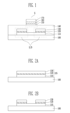
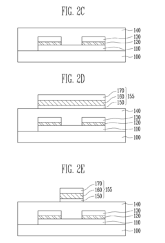
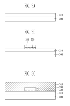
Semiconductor element, method for manufacturing same, and electronic device including same
PatentInactiveUS20100044702A1
Innovation
- A semiconductor element with a polycrystalline ZnO film active layer where impurities, such as sulfur, are added in higher concentrations to the grain boundary regions than to the crystal parts, forming ZnS which raises the trap level within the conduction band, thereby reducing the influence of grain boundaries on carrier operation and improving transistor characteristics like electron field-effect mobility and subthreshold coefficient S.
Transparent transistor and method of manufacturing the same
PatentInactiveUS20100155792A1
Innovation
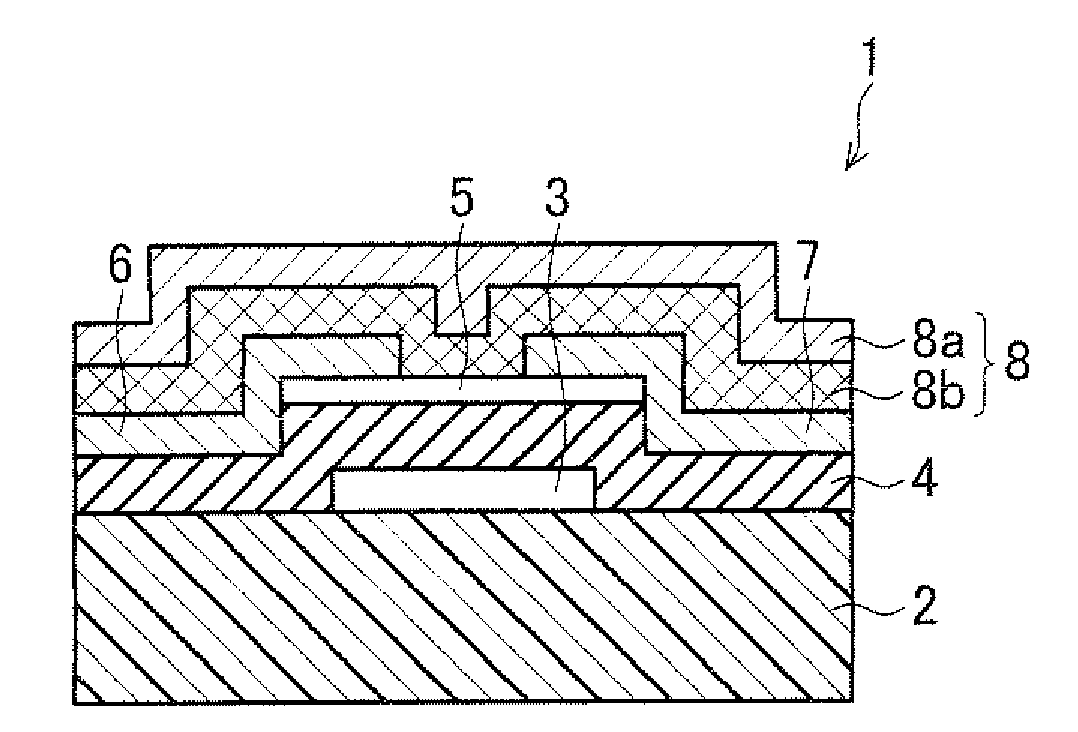
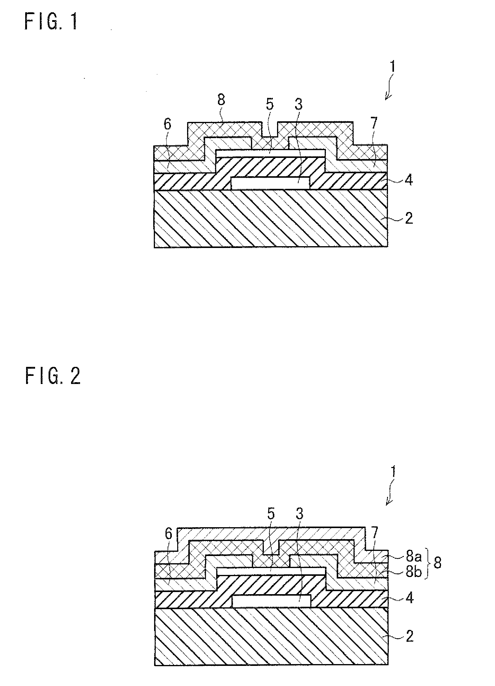
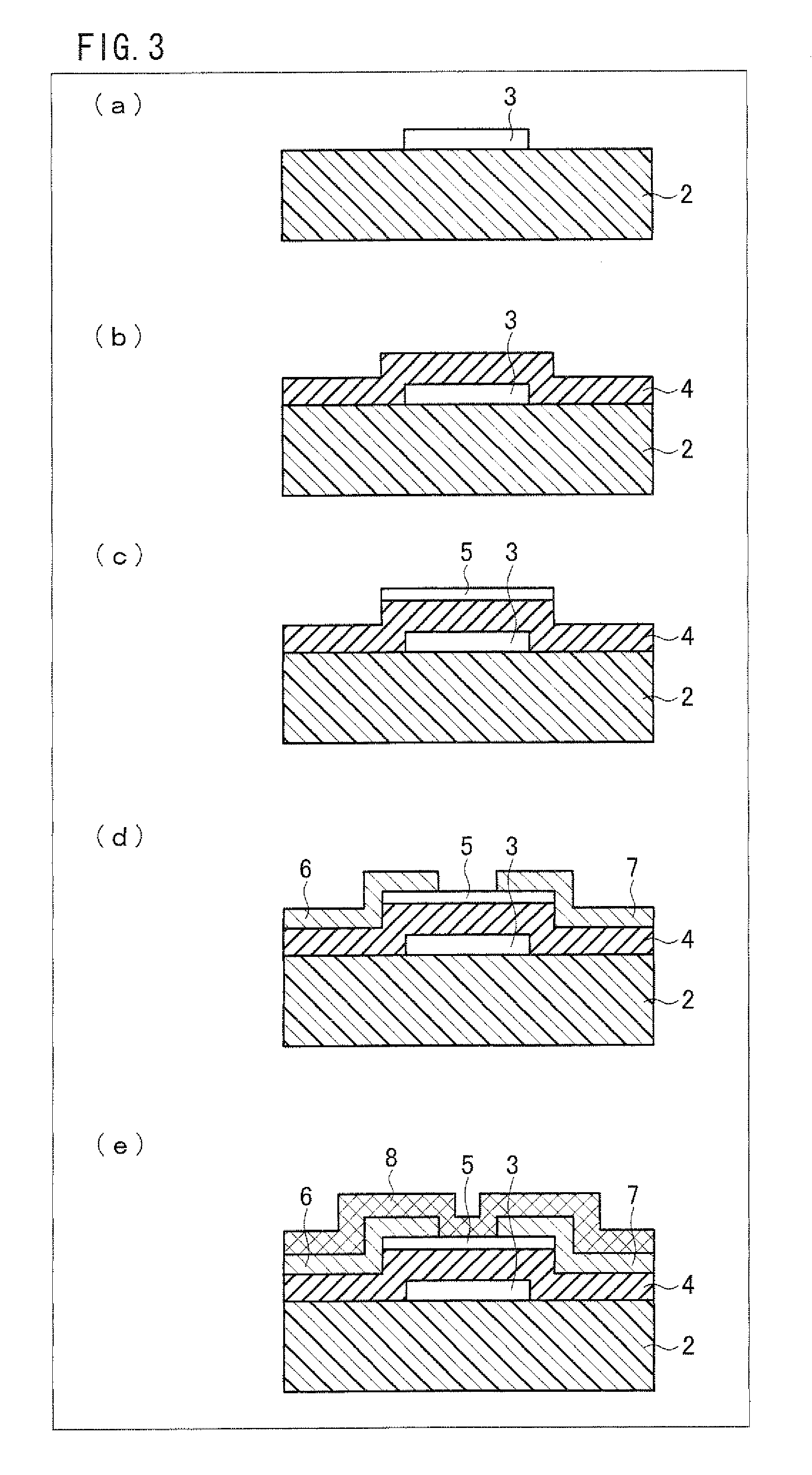
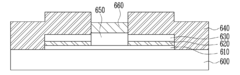
- A stacked structure for transparent transistors is implemented, comprising a substrate with source and drain electrodes having a multi-layered structure of a lower transparent layer, a metal layer, and an upper transparent layer, where the lower and upper transparent layers are formed of the same transparent semiconductor material, and a gate electrode is aligned with the channel, potentially including nitride layers for enhanced refractive index and conductivity.
Materials Science Advancements for Transparent Semiconductor Devices
The evolution of transparent semiconductor materials has been pivotal in advancing transparent transistor technology. Traditional semiconductors like silicon, while efficient, lack optical transparency required for next-generation display and optoelectronic applications. Recent breakthroughs in materials science have focused on wide-bandgap semiconductors, particularly metal oxides such as indium gallium zinc oxide (IGZO), zinc oxide (ZnO), and tin oxide (SnO2), which offer both electrical conductivity and optical transparency.
These oxide semiconductors demonstrate carrier mobilities ranging from 10-50 cm²/Vs, significantly higher than amorphous silicon, while maintaining transparency levels above 80% in the visible spectrum. The crystalline structure of these materials allows for efficient electron transport while minimizing light absorption, creating an ideal balance for transparent electronic applications.
Nanomaterial innovations have further expanded the materials palette for transparent semiconductors. Two-dimensional materials like graphene and transition metal dichalcogenides (TMDs) exhibit exceptional carrier mobility (exceeding 10,000 cm²/Vs for graphene) while maintaining high transparency. However, challenges in bandgap engineering and large-scale production have limited their commercial implementation.
Composite materials represent another significant advancement, combining the benefits of different material classes. Hybrid organic-inorganic structures have shown promise in achieving flexibility alongside transparency and electrical performance. These composites often utilize solution-processing techniques, enabling low-temperature fabrication compatible with flexible substrates.
Doping strategies have evolved to precisely control carrier concentration in transparent semiconductors. Innovations in atomic layer deposition (ALD) and pulsed laser deposition (PLD) techniques allow for atomic-level control of material composition, enabling fine-tuning of electrical properties while preserving optical transparency.
Environmental stability remains a critical challenge for many transparent semiconductor materials. Recent research has focused on developing passivation layers and encapsulation techniques to protect sensitive materials from atmospheric degradation. Additionally, efforts to reduce reliance on scarce elements like indium have led to exploration of alternative compositions using earth-abundant elements.
The interface engineering between different material layers has emerged as a crucial aspect of transparent device performance. Novel surface treatments and interlayer materials have been developed to minimize contact resistance and improve charge transfer across material boundaries, significantly enhancing overall device efficiency and reliability.
Integration Challenges with Existing Display and Electronic Technologies
The integration of transparent transistors with existing display and electronic technologies presents significant technical challenges that must be addressed for successful commercial implementation. Current display technologies rely on established manufacturing processes optimized for conventional transistor materials, creating compatibility issues when introducing transparent alternatives. The primary challenge lies in the thermal budget constraints of existing production lines, as many transparent conducting oxide (TCO) materials require high-temperature processing that may damage underlying display components.
Interface engineering represents another critical hurdle, as the junction between transparent transistors and conventional electronic components often suffers from contact resistance issues and potential electronic band misalignment. These interface problems can significantly degrade device performance and reliability, particularly in applications requiring precise electronic characteristics.
Manufacturing process compatibility presents additional complications, as transparent transistor fabrication may require specialized deposition techniques or etching processes that differ substantially from standard semiconductor manufacturing. The introduction of these new processes necessitates significant modifications to existing production lines, increasing implementation costs and potentially reducing yield rates during the transition period.
Dimensional scaling poses particular difficulties, as transparent transistors must conform to the increasingly fine feature sizes demanded by modern electronics while maintaining their transparency and electrical performance. This challenge becomes especially pronounced in high-resolution display applications where pixel densities continue to increase annually.
Reliability and lifetime considerations further complicate integration efforts. Transparent transistors must demonstrate comparable durability to silicon-based alternatives under various environmental conditions, including resistance to humidity, temperature fluctuations, and mechanical stress. Current transparent semiconductor materials often exhibit performance degradation over time, particularly when exposed to ambient conditions.
Signal integrity and electromagnetic interference (EMI) management represent additional technical challenges. The unique electrical properties of transparent conducting materials can affect signal propagation characteristics, potentially requiring redesigned circuit layouts and shielding approaches to maintain system performance.
Cost considerations ultimately determine commercial viability, as integration solutions must balance technical performance with economic feasibility. While transparent transistors offer compelling advantages for certain applications, their integration costs must decrease substantially through process optimization and economies of scale before widespread adoption becomes realistic across the electronics industry.
Unlock deeper insights with Patsnap Eureka Quick Research — get a full tech report to explore trends and direct your research. Try now!
Generate Your Research Report Instantly with AI Agent
Supercharge your innovation with Patsnap Eureka AI Agent Platform!