Technical Insights into Transparent Transistor Conductive Polymers
OCT 21, 202510 MIN READ
Generate Your Research Report Instantly with AI Agent
PatSnap Eureka helps you evaluate technical feasibility & market potential.
Transparent Transistor Evolution and Objectives
Transparent transistor technology has evolved significantly over the past four decades, transitioning from traditional silicon-based semiconductors to novel materials that combine optical transparency with electrical conductivity. The journey began in the 1980s with the development of amorphous silicon thin-film transistors (TFTs), which offered limited transparency but established the foundation for future innovations. The 1990s witnessed the emergence of metal oxide semiconductors, particularly indium gallium zinc oxide (IGZO), which demonstrated superior electron mobility while maintaining reasonable transparency levels.
A paradigm shift occurred in the early 2000s with the introduction of conductive polymers as viable materials for transparent transistor applications. These organic materials offered unprecedented flexibility and processing advantages compared to their inorganic counterparts. The development of poly(3,4-ethylenedioxythiophene) polystyrene sulfonate (PEDOT:PSS) marked a significant milestone, as it combined good electrical conductivity with optical transparency exceeding 80% in the visible spectrum.
The 2010s saw rapid advancement in polymer chemistry and device engineering, leading to conductive polymers with enhanced charge carrier mobility and environmental stability. Researchers focused on optimizing molecular structures and developing novel synthesis methods to improve the performance-transparency trade-off that had historically limited polymer-based transistors. Concurrently, hybrid approaches combining polymers with nanomaterials such as graphene and carbon nanotubes emerged as promising strategies to overcome inherent limitations of purely organic systems.
Current technological objectives in transparent transistor development center around achieving higher charge carrier mobility while maintaining optical transparency above 90%. Researchers aim to develop conductive polymers with mobility values exceeding 10 cm²/Vs, approaching the performance of amorphous silicon while retaining the advantages of solution processability and mechanical flexibility. Another critical goal involves enhancing environmental stability, as many high-performance conductive polymers remain susceptible to degradation when exposed to oxygen and moisture.
Looking forward, the field is moving toward multifunctional transparent transistors that integrate sensing capabilities, energy harvesting, and self-healing properties. These advanced devices will require conductive polymers with precisely engineered band structures and interfacial properties. The ultimate objective is to enable fully transparent, flexible electronic systems that can be manufactured using low-cost, large-area processing techniques such as roll-to-roll printing.
Industry stakeholders anticipate that achieving these technological objectives will revolutionize applications in transparent displays, smart windows, wearable electronics, and augmented reality interfaces. The convergence of high performance, optical transparency, mechanical flexibility, and cost-effective manufacturing represents the north star guiding research efforts in this rapidly evolving field.
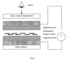
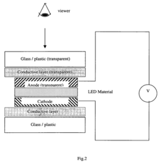
Market Applications for Transparent Electronics
Transparent electronics represent a revolutionary frontier in technology, offering unprecedented opportunities across multiple industries. The integration of transparent transistor conductive polymers has catalyzed significant market applications that extend beyond traditional electronics. These applications leverage the unique combination of electrical conductivity and optical transparency that these materials provide.
The consumer electronics sector has emerged as a primary beneficiary of transparent electronics technology. Smartphones and tablets now incorporate transparent touch panels that offer enhanced user experience while maintaining aesthetic appeal. Major manufacturers have begun implementing transparent displays that enable augmented reality features without compromising device design. This market segment is experiencing rapid growth as consumers increasingly demand devices that seamlessly blend technology with everyday life.
Automotive applications represent another substantial market opportunity. Heads-up displays utilizing transparent electronics allow drivers to access critical information without diverting attention from the road. Advanced driver-assistance systems increasingly incorporate transparent sensors and displays integrated into windshields and windows. The automotive industry's shift toward autonomous vehicles further amplifies demand for transparent electronics that can be unobtrusively embedded throughout vehicle interiors.
The architectural and construction industry has adopted transparent electronics for smart windows and building facades. These applications enable dynamic control of light transmission and energy efficiency while maintaining aesthetic qualities. Commercial buildings equipped with transparent solar cells integrated into windows generate electricity while preserving natural lighting. This dual functionality addresses growing demands for sustainable building solutions without sacrificing design considerations.
Healthcare applications of transparent electronics include wearable medical devices that monitor vital signs while remaining virtually invisible on the skin. Transparent biosensors offer continuous health monitoring capabilities with minimal patient discomfort. Hospitals have begun implementing transparent display technologies for patient information systems that enhance the clinical environment while improving information accessibility.
Military and aerospace sectors utilize transparent electronics for advanced heads-up displays in aircraft and combat vehicles. These applications provide critical information to operators while maintaining optimal visibility. Transparent radar and communication systems integrated into vehicle windows reduce equipment footprint while enhancing functionality.
The retail industry has embraced transparent display technologies for interactive storefronts and product showcases. These applications create immersive shopping experiences while preserving visibility of physical merchandise. Smart mirrors incorporating transparent electronics enable virtual try-on experiences that blend digital content with physical reality.
As manufacturing capabilities advance and costs decrease, transparent electronics applications continue to expand into new markets, driving innovation across industries and creating significant opportunities for technology developers and implementers.
Current Status and Barriers in Conductive Polymer Technology
Conductive polymers have emerged as a promising alternative to traditional inorganic materials in transparent transistor applications, with significant advancements achieved over the past decade. Currently, the field has reached a stage where laboratory demonstrations show impressive performance metrics, with conductivities approaching 4,000 S/cm for certain polymer systems like PEDOT:PSS after secondary doping treatments. Transparency levels exceeding 90% in the visible spectrum have been achieved for thin films, making these materials viable candidates for transparent electronics.
Despite these achievements, several critical barriers impede widespread commercial adoption. The most significant challenge remains the trade-off between conductivity and transparency. As film thickness increases to improve conductivity, optical transparency inevitably decreases, creating a fundamental limitation that requires innovative molecular design approaches to overcome. This relationship follows a non-linear pattern that becomes increasingly problematic at higher conductivity requirements.
Stability issues present another major hurdle, with many high-performance conductive polymers exhibiting performance degradation under ambient conditions. Oxygen and moisture sensitivity leads to conductivity losses of up to 40% within weeks of exposure in some systems. UV stability also remains problematic, with photooxidation mechanisms causing chain scission and loss of conjugation in the polymer backbone. These degradation pathways significantly limit device lifetimes compared to inorganic alternatives.
Processing challenges further complicate industrial implementation. Many high-performance conductive polymers require toxic solvents like chloroform or dichlorobenzene for solution processing, creating environmental and safety concerns for mass production. Additionally, batch-to-batch variations in molecular weight distribution and doping levels lead to inconsistent performance metrics, with conductivity variations of ±15% commonly observed between production runs.
The cost structure of conductive polymer production presents economic barriers to market entry. Current synthesis routes for high-performance materials involve multiple steps with expensive catalysts and purification procedures. Production costs for specialized transparent conductive polymers range from $500-2,000/kg, significantly higher than established transparent conductors like ITO. This cost differential makes economic justification difficult without substantial performance advantages.
Geographically, research and development in this field shows distinct patterns. North America and Europe lead in fundamental polymer chemistry innovations, while East Asian countries, particularly South Korea and Japan, dominate in device integration and manufacturing scale-up. China has rapidly increased its patent filings in this area, growing at approximately 25% annually over the past five years, suggesting an emerging competitive landscape with regional specialization in different aspects of the technology value chain.
Contemporary Approaches to Polymer Conductivity Enhancement
01 Conductive polymer compositions with enhanced transparency
Specific formulations of conductive polymers can be designed to maximize optical transparency while maintaining electrical conductivity. These compositions typically involve careful control of polymer chain length, dopant concentration, and processing conditions to minimize light scattering. Advanced synthesis methods can produce polymers with ordered structures that allow for high transparency in the visible light spectrum while preserving conductive pathways for electron transport.- Conductive polymer compositions with enhanced transparency: Specific formulations of conductive polymers can be designed to enhance transparency while maintaining electrical conductivity. These compositions often involve careful control of polymer chain length, molecular weight distribution, and processing conditions. By optimizing these parameters, the light scattering within the polymer matrix can be minimized, resulting in higher optical transparency. These transparent conductive polymers find applications in displays, touch screens, and optoelectronic devices.
- Transparent conductive polymer films fabrication techniques: Various fabrication techniques can be employed to produce transparent conductive polymer films with optimized optical properties. These methods include solution processing, spin coating, spray coating, and roll-to-roll manufacturing. The processing conditions, such as solvent selection, drying temperature, and post-treatment steps, significantly influence the transparency of the resulting films. Advanced deposition techniques can create uniform thin films with minimal defects, enhancing both conductivity and transparency.
- Polymer blends and composites for improved transparency: Blending conductive polymers with other materials can enhance transparency while maintaining electrical properties. These composites often incorporate transparent insulating polymers, nanofillers, or other additives that improve optical clarity. The strategic combination of different polymers with complementary properties allows for the fine-tuning of both electrical conductivity and optical transparency. The morphology control of these blends is crucial for achieving the desired balance between transparency and conductivity.
- Doping strategies to enhance transparency in conductive polymers: Various doping approaches can be used to improve the transparency of conductive polymers. Chemical dopants, counter-ions, and secondary dopants can be selected to minimize light absorption while enhancing charge carrier mobility. The doping level and distribution within the polymer matrix significantly affect both the electrical and optical properties. Controlled doping processes can reduce visible light absorption while maintaining the necessary charge transport properties for electrical conductivity.
- Nanostructured transparent conductive polymer systems: Incorporating nanostructures into conductive polymers can significantly enhance transparency. These systems include polymer nanofibers, nanoporous structures, and hierarchical architectures that reduce light scattering while providing conductive pathways. Nanoscale engineering of polymer morphology allows for the creation of materials with high optical clarity and electrical conductivity. These nanostructured systems often exhibit improved mechanical flexibility and stability compared to conventional transparent conductive materials.
02 Transparent electrode applications using conductive polymers
Conductive polymers with high transparency are utilized in various electronic devices as transparent electrodes. These applications include touchscreens, displays, solar cells, and flexible electronics. The polymers provide advantages over traditional transparent conductors like indium tin oxide (ITO), including flexibility, lower cost, and compatibility with roll-to-roll processing. The transparency and conductivity can be tuned to meet specific application requirements through modification of the polymer structure.Expand Specific Solutions03 Nanocomposite approaches for transparent conductive materials
Incorporating nanomaterials such as carbon nanotubes, graphene, or metal nanowires into conductive polymer matrices can significantly enhance both transparency and conductivity. These nanocomposites benefit from the synergistic effects of the polymer matrix and the nanofiller, where the polymer provides processability and film-forming properties while the nanomaterial creates efficient conductive networks. The nanofillers can be dispersed at concentrations low enough to maintain high optical transparency while forming percolation networks for electrical conductivity.Expand Specific Solutions04 Processing techniques to improve transparency of conductive polymers
Various processing methods can enhance the transparency of conductive polymers, including solution processing, spin coating, and specialized annealing techniques. These methods control the morphology and crystallinity of the polymer films, which directly impacts their optical properties. Post-treatment processes such as acid treatment or solvent washing can remove excess dopants or impurities that might otherwise reduce transparency. Controlling film thickness and uniformity is also crucial for achieving optimal transparency while maintaining adequate conductivity.Expand Specific Solutions05 Chemical modifications for transparency enhancement
Chemical modifications to the polymer backbone or side chains can significantly improve transparency while preserving conductivity. These modifications include the incorporation of solubilizing groups, adjustment of conjugation length, and strategic placement of substituents that reduce interchain interactions. Some approaches involve copolymerization with transparent monomers or the use of specific dopants that minimize light absorption in the visible spectrum. These chemical strategies can be tailored to achieve specific transparency targets while maintaining the desired level of electrical conductivity.Expand Specific Solutions
Leading Organizations in Transparent Transistor Research
The transparent transistor conductive polymer technology market is in an early growth phase, characterized by significant R&D investments but limited commercial deployment. The global market size is estimated to reach approximately $2-3 billion by 2025, driven by increasing demand for flexible electronics and displays. From a technological maturity perspective, the field remains in development with key players at different stages: academic institutions (MIT, Northwestern University) focus on fundamental research; electronics giants (Samsung Display, BOE Technology, Canon) are advancing practical applications; while specialty materials companies (TDK, Solvay, Mitsubishi Gas Chemical) are developing commercial-grade polymers. Government research organizations like ETRI and Japan Science & Technology Agency are bridging fundamental science with industrial applications, creating a competitive landscape where collaboration and intellectual property protection are equally important.
Electronics & Telecommunications Research Institute
Technical Solution: ETRI has developed advanced transparent transistor technologies based on hybrid organic-inorganic materials. Their flagship approach combines solution-processed metal oxide semiconductors (primarily indium-gallium-zinc-oxide, IGZO) with specially engineered conductive polymers for electrodes and interconnects. ETRI's proprietary "TOPS" (Transparent Organic-Polymer Semiconductor) platform achieves mobility values exceeding 15 cm²/Vs while maintaining transparency above 85% across the visible spectrum. Their innovative low-temperature annealing process (max 200°C) enables fabrication on flexible plastic substrates while ensuring high device performance and stability. ETRI researchers have pioneered multilayer architectures that optimize the interface between different functional layers, resulting in transistors with on/off ratios exceeding 10^8 and threshold voltages below 0.5V. The institute has successfully demonstrated these technologies in prototype applications including transparent displays, wearable electronics, and smart windows. Their recent advancements include self-healing polymer composites that can recover from mechanical damage, enhancing the durability of flexible transparent electronics for real-world applications.
Strengths: Excellent balance of high performance and processability; compatibility with existing display manufacturing infrastructure; superior environmental stability compared to purely organic systems. Weaknesses: Some materials require controlled atmosphere processing; performance variability across large-area substrates; higher cost compared to conventional silicon-based technologies.
Oregon State University
Technical Solution: Oregon State University has developed innovative transparent transistor technologies based on amorphous oxide semiconductors (AOS) combined with conductive polymers. Their hybrid approach integrates zinc tin oxide (ZTO) as the semiconductor channel with PEDOT:PSS as transparent conductive electrodes. This combination leverages the high mobility of oxide semiconductors (typically 10-30 cm²/Vs) with the flexibility and solution processability of conductive polymers. OSU researchers have pioneered low-temperature processing methods (<200°C) that enable deposition on plastic substrates, creating fully transparent and flexible transistors with on/off ratios exceeding 10^7. Their proprietary interface engineering techniques minimize contact resistance between the polymer electrodes and oxide semiconductor layers, resulting in devices with threshold voltages below 1V and subthreshold swing values approaching the theoretical limit of 60 mV/decade. The university has demonstrated these technologies in functional prototypes including transparent displays, RFID tags, and sensor arrays with exceptional performance stability under mechanical deformation (bending radii <5mm) and after thousands of bending cycles.
Strengths: Excellent combination of high mobility from oxide semiconductors with flexibility from polymers; low-temperature processing compatible with roll-to-roll manufacturing; superior operational stability compared to purely organic systems. Weaknesses: Interface engineering between dissimilar materials remains challenging; some performance variability between batches; limited long-term stability under extreme environmental conditions.
Breakthrough Patents in Transparent Conductive Polymers
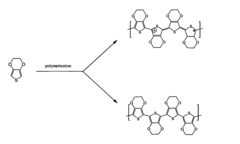
Highly conducting and transparent thin polymer films formed from double and multiple layers of poly(3,4-ethylenedioxythiopene) and its derivatives
PatentInactiveUS7026042B2
Innovation
- A method involving the formation of multilayer conductive polymer films using poly(3,4-ethylenedioxythiophene) derivatives through a spin-coating and heating process, where multiple thin layers are sequentially polymerized on a substrate, optimizing conductivity and transparency by varying process parameters like spin speed, temperature, and molar ratios.
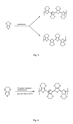
Method for manufacturing conductive polymer thin film having semiconductor characteristic and thin-film transistor comprising conductive polymer thin film having semiconductor characteristic
PatentActiveUS20200212305A1
Innovation
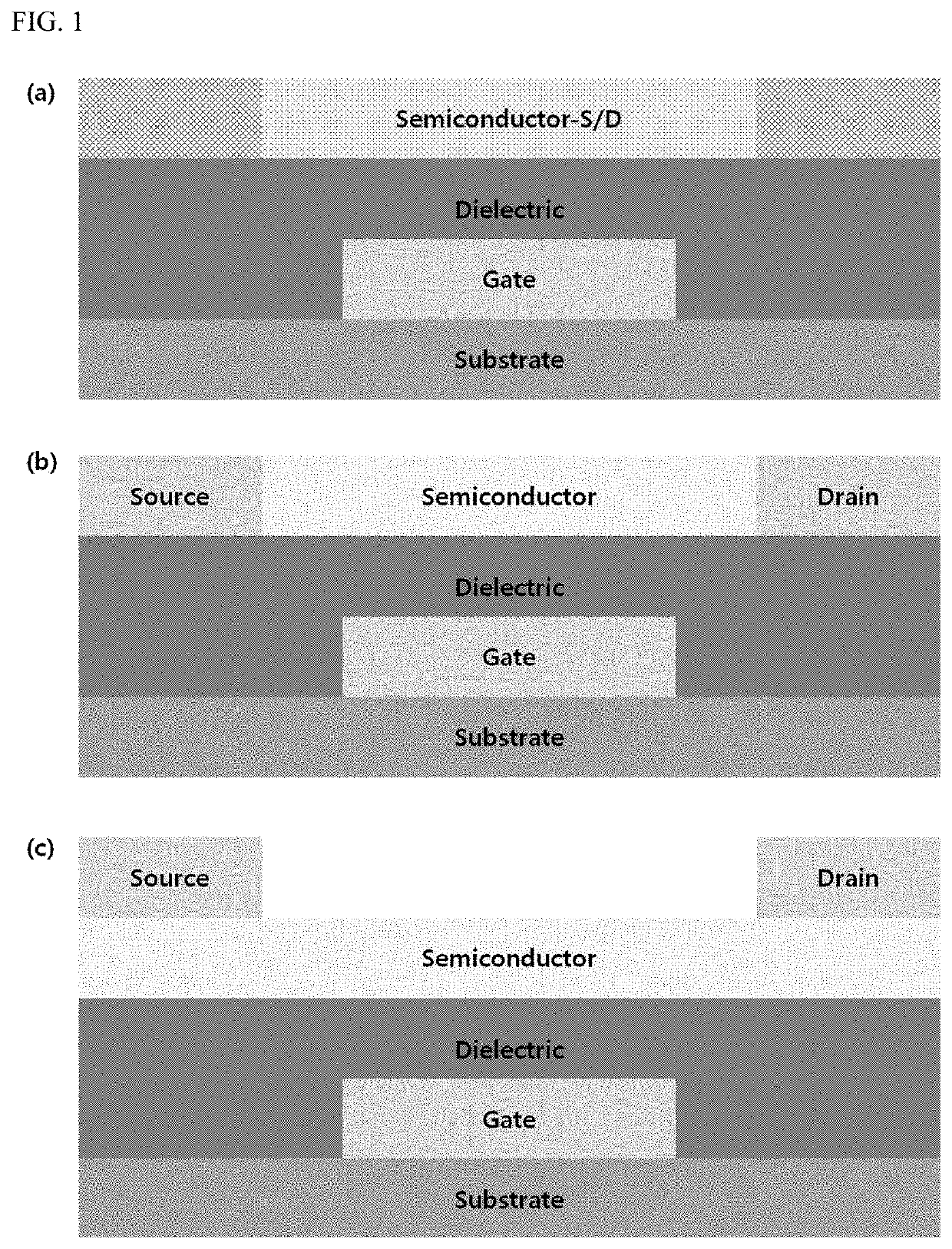
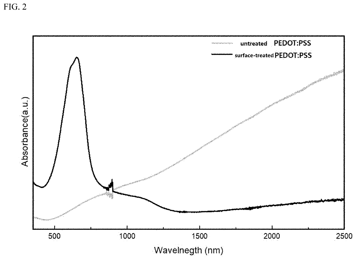
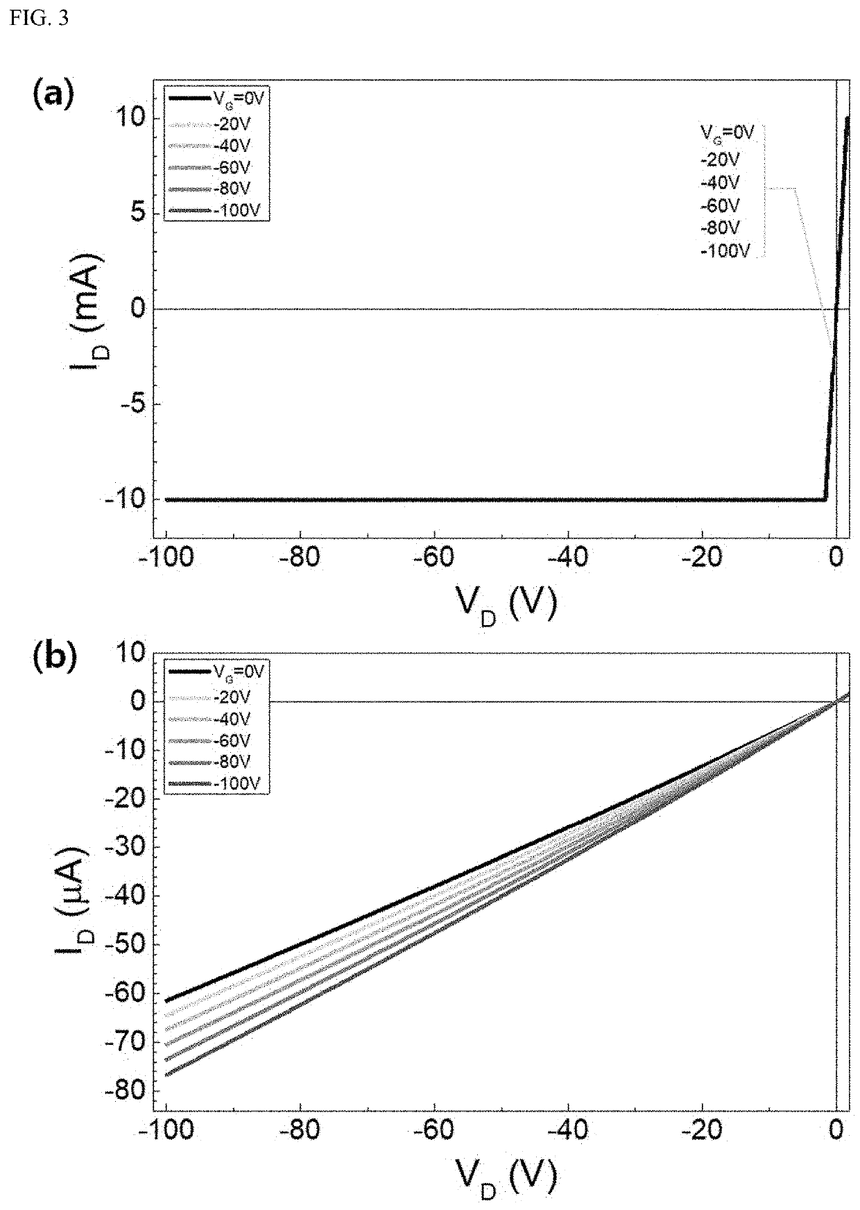
- A method for manufacturing a transparent conductive polymer thin-film with semiconductor properties is developed, where a conductive polymer thin-film is treated with a surface treatment agent to reduce charge density, allowing it to function as both a semiconductor and electrode layer, thereby minimizing light loss and eliminating the need for separate metal electrodes.
Manufacturing Scalability Considerations
The scalability of manufacturing processes represents a critical factor in the commercial viability of transparent transistor conductive polymers. Current laboratory-scale synthesis methods often involve complex procedures that are difficult to translate to industrial production. Solution processing techniques, including spin-coating, inkjet printing, and roll-to-roll processing, offer promising pathways for large-scale manufacturing but face significant challenges in maintaining consistent film thickness and morphology across large areas.
Material purity requirements present another substantial hurdle for manufacturing scalability. Industrial-grade production demands stringent quality control measures to ensure batch-to-batch consistency, as even minor impurities can dramatically affect the electrical properties of conductive polymers. The development of robust purification protocols that can be implemented at scale without prohibitive cost increases remains an active area of research.
Thermal stability during processing represents a significant consideration for manufacturing integration. Many conductive polymers exhibit sensitivity to elevated temperatures, which can limit their compatibility with standard semiconductor fabrication processes. Engineering polymers with enhanced thermal resilience or developing low-temperature processing alternatives will be essential for seamless integration with existing manufacturing infrastructure.
Environmental considerations also impact manufacturing scalability. Traditional synthesis routes often involve hazardous solvents and reagents that pose challenges for worker safety and environmental compliance. The transition toward greener chemistry approaches, utilizing less toxic solvents and more environmentally benign reaction pathways, is gaining momentum but requires further optimization to maintain performance metrics while improving sustainability profiles.
Cost factors ultimately determine commercial feasibility. Current production costs for high-performance conductive polymers remain significantly higher than conventional semiconductor materials, primarily due to complex synthesis procedures and expensive precursors. Economies of scale have not yet been fully realized in this domain, though recent advances in synthetic methodologies suggest pathways toward cost reduction. Simplified synthetic routes with fewer reaction steps and higher yields represent a promising direction for improving economic viability.
Equipment compatibility presents another dimension of manufacturing scalability. Integration with existing semiconductor fabrication lines requires conductive polymer processes to be compatible with standard equipment. Developing deposition techniques that can utilize modified versions of conventional tools rather than requiring entirely new manufacturing infrastructure would significantly accelerate industrial adoption and reduce capital investment barriers.
Environmental Impact and Sustainability Factors
The development and adoption of transparent transistor conductive polymers present significant environmental implications that warrant careful consideration. These materials offer potential sustainability advantages over traditional inorganic semiconductors, particularly in terms of resource efficiency. Conductive polymers typically require less energy-intensive manufacturing processes compared to silicon-based technologies, which demand high temperatures and ultra-clean environments. This reduced energy footprint translates to lower carbon emissions during production phases.
Furthermore, many conductive polymers can be synthesized from renewable resources, presenting an opportunity to decrease dependence on finite mineral resources. The potential for bio-based precursors derived from agricultural byproducts or sustainable forestry practices could establish a more environmentally responsible supply chain for electronics manufacturing. This shift aligns with circular economy principles and reduces extraction pressures on critical minerals.
Waste management considerations also favor conductive polymer technologies. Unlike conventional electronics containing heavy metals and toxic compounds, properly designed conductive polymers can be formulated to minimize hazardous substances. Some research indicates potential biodegradability pathways for certain polymer structures, though this remains an active area requiring further development before commercial implementation.
Water consumption represents another environmental dimension where transparent conductive polymers may offer advantages. Traditional semiconductor fabrication consumes substantial quantities of ultra-pure water, whereas polymer processing typically requires significantly less. This benefit becomes increasingly relevant as water scarcity affects more regions globally.
However, challenges remain regarding the environmental profile of these materials. Solvent usage in polymer processing can introduce toxicity concerns if not properly managed. Additionally, the environmental persistence of some polymer additives and stabilizers requires thorough assessment. Life cycle analyses indicate that while production impacts may be lower, end-of-life management remains problematic without dedicated recycling infrastructure.
The scalability of environmentally optimized production methods presents another hurdle. Laboratory-scale synthesis often employs green chemistry principles that prove difficult to maintain at industrial scales. Bridging this gap requires focused research on sustainable manufacturing techniques that preserve environmental benefits while meeting commercial production requirements.
As transparent transistor conductive polymer technologies mature, integrating environmental considerations into material design and manufacturing processes will be crucial for maximizing their sustainability potential. This proactive approach can help position these materials as environmentally preferable alternatives in the expanding market for transparent electronics.
Unlock deeper insights with PatSnap Eureka Quick Research — get a full tech report to explore trends and direct your research. Try now!
Generate Your Research Report Instantly with AI Agent
Supercharge your innovation with PatSnap Eureka AI Agent Platform!