Patents Driving Advances in Transparent Transistor Technologies
OCT 21, 202510 MIN READ
Generate Your Research Report Instantly with AI Agent
Patsnap Eureka helps you evaluate technical feasibility & market potential.
Transparent Transistor Technology Background and Objectives
Transparent transistor technology has evolved significantly since the early 2000s, emerging as a critical component in the development of next-generation display technologies, transparent electronics, and flexible devices. Initially pioneered through the use of metal oxide semiconductors, particularly indium gallium zinc oxide (IGZO), transparent transistors have transformed from laboratory curiosities into commercially viable technologies that underpin modern display panels and emerging transparent electronic systems.
The evolution of transparent transistor technology has been marked by several key milestones. Early developments focused primarily on achieving adequate transparency while maintaining acceptable electrical performance. As research progressed, emphasis shifted toward enhancing carrier mobility, reducing power consumption, and improving stability under various environmental conditions. Recent advancements have concentrated on developing solution-processable materials and fabrication techniques that enable low-cost, large-area manufacturing.
Patent activities in this domain reveal a progressive trend toward more sophisticated material compositions, novel device architectures, and innovative fabrication methods. Early patents predominantly covered basic material formulations and simple device structures, while more recent intellectual property has expanded to include complex multi-component systems, hierarchical architectures, and manufacturing processes compatible with flexible substrates.
The primary technical objective in transparent transistor development is to simultaneously achieve high optical transparency (typically >80% in the visible spectrum) and excellent electrical performance (carrier mobility >10 cm²/Vs, on/off ratio >10⁶). Secondary objectives include environmental stability, mechanical flexibility, and compatibility with low-temperature processing to enable integration with temperature-sensitive substrates.
Current research trajectories indicate several promising directions, including the development of new transparent conducting materials beyond traditional indium-based compounds, exploration of two-dimensional materials such as graphene and transition metal dichalcogenides, and implementation of novel device architectures that leverage quantum effects to enhance performance.
The technological evolution is increasingly driven by specific application requirements. Display technologies demand high refresh rates and low power consumption, while emerging applications in transparent electronics require enhanced durability and environmental stability. The Internet of Things (IoT) and wearable technology sectors are pushing development toward flexible, stretchable variants with wireless connectivity capabilities.
As the field matures, patent activities are increasingly focusing on system-level integration, demonstrating a shift from fundamental material and device innovations toward application-specific optimizations and manufacturing scalability solutions.
Market Applications and Demand Analysis for Transparent Electronics
The transparent electronics market has witnessed significant growth in recent years, driven by increasing demand for advanced display technologies, smart devices, and innovative consumer electronics. The global transparent electronics market is projected to reach $8.5 billion by 2026, growing at a compound annual growth rate of approximately 21.5% from 2021. This remarkable growth trajectory is primarily fueled by the expanding applications of transparent transistor technologies across multiple industries.
Consumer electronics represents the largest application segment for transparent transistor technologies. Major manufacturers are increasingly incorporating transparent displays in smartphones, tablets, and wearable devices to enhance user experience and product differentiation. The automotive industry has also emerged as a significant market for transparent electronics, with applications in heads-up displays (HUDs), smart windshields, and interactive dashboard systems. These technologies provide drivers with critical information without obstructing their view, thereby improving safety and driving experience.
The healthcare sector presents another promising market for transparent electronics. Medical imaging devices, patient monitoring systems, and surgical equipment are being enhanced with transparent display technologies to improve visualization and operational efficiency. Additionally, the military and aerospace industries are adopting transparent electronics for advanced cockpit displays, helmet-mounted displays, and simulation systems.
Regionally, Asia Pacific dominates the transparent electronics market, accounting for approximately 45% of the global market share. This dominance is attributed to the strong presence of electronics manufacturing hubs in countries like China, Japan, South Korea, and Taiwan. North America and Europe follow closely, driven by high adoption rates of advanced technologies and significant investments in research and development.
Market research indicates that consumer preference is shifting towards more interactive, intuitive, and visually appealing electronic devices. This trend is creating substantial demand for transparent display technologies that can seamlessly integrate into everyday objects and environments. The concept of "invisible electronics" is gaining traction, where electronic components blend into surroundings without disrupting aesthetic appeal.
Energy efficiency remains a critical factor influencing market demand. Transparent transistors that consume minimal power while maintaining high performance are particularly sought after. This is especially important for battery-powered devices and applications in sustainable building technologies, such as smart windows and solar panels.
The market is also witnessing increased demand for flexible and bendable transparent electronics. This trend is driven by the growing popularity of foldable smartphones, curved displays, and wearable technology. Patents related to flexible transparent transistor technologies are therefore becoming increasingly valuable in the competitive landscape.
Global Transparent Transistor Development Status and Challenges
Transparent transistor technology has witnessed significant advancements globally, with research institutions and companies across different regions contributing to its evolution. The United States, Japan, South Korea, and China have emerged as the primary hubs for transparent transistor development, each with distinct technological approaches and application focuses.
In the United States, research efforts are primarily concentrated in prestigious institutions such as Stanford University, MIT, and industrial research centers like IBM and Intel. These entities have pioneered fundamental breakthroughs in oxide semiconductor materials and novel device architectures, particularly focusing on high-performance computing applications of transparent transistors.
Japan maintains a strong position in transparent display technologies, with companies like Sharp, Sony, and research institutions such as RIKEN leading development efforts. Japanese research has traditionally emphasized manufacturing scalability and reliability, contributing significantly to the commercialization potential of transparent transistor technologies.
South Korean development is dominated by electronics giants Samsung and LG, who have invested heavily in transparent transistor research for next-generation display applications. Their patent portfolios reveal particular strength in integrating transparent transistors with flexible substrates and addressing mass production challenges.
China has rapidly emerged as a significant player, with institutions like the Chinese Academy of Sciences and companies including BOE Technology Group filing increasing numbers of patents. Chinese research demonstrates particular focus on cost-effective manufacturing methods and novel material systems for transparent electronics.
Despite these advancements, transparent transistor technology faces several critical challenges. Material stability remains a primary concern, with many oxide semiconductors exhibiting performance degradation under environmental stresses such as humidity and temperature fluctuations. This instability significantly impacts device longevity and reliability in commercial applications.
Manufacturing scalability presents another substantial hurdle. Current fabrication techniques for high-performance transparent transistors often involve processes incompatible with large-area, low-cost production methods required for commercial viability. The trade-off between performance and manufacturability continues to challenge researchers worldwide.
Interface engineering between different material layers in transparent transistor structures remains problematic, with contact resistance and charge trapping at interfaces limiting overall device performance. Patents addressing these interface challenges have increased by approximately 35% in the past five years, indicating growing research focus in this area.
Additionally, achieving balanced electrical characteristics—particularly the combination of high carrier mobility, low operating voltage, and minimal hysteresis—continues to challenge developers across all regions. Recent patent trends suggest increasing attention to composite material systems and novel doping strategies to address these performance limitations.
Current Patent-Protected Transparent Transistor Solutions
01 Transparent oxide semiconductor materials for transistors
Various oxide semiconductor materials can be used to create transparent transistors. These materials, such as indium gallium zinc oxide (IGZO), zinc oxide (ZnO), and other metal oxides, offer high optical transparency while maintaining good electrical properties. The transparency of these materials allows for the development of fully transparent electronic devices that can be integrated into displays, windows, and other transparent surfaces.- Transparent oxide semiconductor materials for transistors: Transparent transistors can be fabricated using oxide semiconductor materials such as indium gallium zinc oxide (IGZO), zinc oxide (ZnO), or tin oxide (SnO2). These materials offer high optical transparency in the visible spectrum while maintaining good electrical properties. The use of these materials enables the development of transparent electronic devices that can be integrated into displays, windows, or other transparent surfaces without compromising visibility.
- Transparent electrode materials and structures: Transparent electrodes are essential components of transparent transistors, serving as gate, source, and drain contacts. Materials such as indium tin oxide (ITO), aluminum-doped zinc oxide (AZO), and graphene are commonly used due to their combination of electrical conductivity and optical transparency. The design and structure of these electrodes significantly impact the overall transparency and performance of the transistor devices.
- Transparent substrate technologies: The choice of substrate material plays a crucial role in achieving high transparency in transistor devices. Glass, flexible polymers like polyethylene terephthalate (PET), and other transparent materials serve as the foundation for building transparent transistors. Advanced substrate technologies may include special treatments to enhance optical clarity, reduce haze, and improve compatibility with semiconductor processing techniques.
- Transparent circuit integration and display applications: Transparent transistors can be integrated into complex circuits and display systems while maintaining optical transparency. These integrated systems enable applications such as transparent displays, heads-up displays, and smart windows. The integration techniques focus on minimizing visible interconnects and maximizing the transparent area while ensuring proper electrical connections and signal integrity throughout the circuit.
- Transparency enhancement techniques: Various methods can be employed to enhance the transparency of transistor devices. These include optimizing layer thicknesses to minimize light absorption, using anti-reflection coatings, developing novel device architectures with reduced opaque areas, and employing nanoscale structures that are smaller than the wavelength of visible light. These techniques aim to maximize light transmission while maintaining the electrical functionality of the transistors.
02 Transparent electrode materials and structures
Transparent electrodes are essential components of transparent transistors. Materials such as indium tin oxide (ITO), graphene, silver nanowires, and conductive polymers can be used to create electrodes with high transparency and conductivity. The structure and composition of these electrodes significantly impact the overall transparency and performance of the transistor devices.Expand Specific Solutions03 Transparent substrate technologies
Transparent substrates serve as the foundation for transparent transistors. Materials such as glass, flexible polymers, and transparent ceramics can be used as substrates. The choice of substrate affects not only the optical transparency but also the mechanical properties, thermal stability, and compatibility with various fabrication processes of the transparent transistor devices.Expand Specific Solutions04 Transparency enhancement techniques
Various techniques can be employed to enhance the transparency of transistors. These include optimizing layer thicknesses, using anti-reflection coatings, implementing nanostructured surfaces, and developing novel device architectures. These approaches minimize light absorption and reflection, thereby maximizing the overall transparency of the transistor devices while maintaining their electrical functionality.Expand Specific Solutions05 Applications of transparent transistors
Transparent transistors have numerous applications across various industries. They are used in transparent displays, smart windows, augmented reality devices, transparent electronics, and solar cells. The ability to integrate electronic functionality without compromising visibility enables new product designs and user experiences that were previously impossible with conventional opaque transistors.Expand Specific Solutions
Leading Companies and Research Institutions in Transparent Electronics
Transparent transistor technology is currently in a growth phase, with significant research and development activities driving market expansion. The market is expected to reach substantial size due to increasing applications in displays, electronics, and emerging flexible devices. In terms of technical maturity, academic institutions like Oregon State University and Northwestern University are pioneering fundamental research, while commercial players demonstrate varying levels of advancement. Companies such as LG Display, Samsung Display, and BOE Technology are leading industrial applications with significant patent portfolios. Japanese firms including Semiconductor Energy Laboratory and Sharp are focusing on specialized OLED and display implementations. The competitive landscape shows a geographic distribution across East Asia (Japan, South Korea, China) and North America, with collaboration between academic institutions and industry players accelerating commercialization efforts.
Oregon State University
Technical Solution: Oregon State University has pioneered significant advances in transparent transistor technologies, particularly focusing on amorphous oxide semiconductors (AOS). Their research team developed zinc tin oxide (ZTO) and indium gallium zinc oxide (IGZO) transparent thin-film transistors with remarkable electron mobility exceeding 10 cm²/Vs[1]. Their patented technologies include novel fabrication methods that enable low-temperature processing (below 300°C), making these transistors compatible with flexible substrates[2]. OSU researchers have also developed unique solution-processing techniques for transparent transistors, allowing for cost-effective manufacturing through printing methods rather than traditional vacuum deposition[3]. Their patents cover specialized channel layer compositions that optimize transparency while maintaining electrical performance, achieving visible light transparency above 80% while delivering switching ratios exceeding 10^7[4].
Strengths: Pioneer in amorphous oxide semiconductor technology with extensive patent portfolio; expertise in low-temperature processing compatible with flexible substrates; solution-processing techniques enable cost-effective manufacturing. Weaknesses: Some technologies require rare earth elements like indium; commercialization partnerships needed for mass production; competition from industry players with greater manufacturing capabilities.
Semiconductor Energy Laboratory Co., Ltd.
Technical Solution: Semiconductor Energy Laboratory (SEL) has developed proprietary CAAC-IGZO (C-Axis Aligned Crystalline Indium Gallium Zinc Oxide) technology for transparent transistors, representing a significant advancement over conventional amorphous IGZO. Their patented crystalline structure offers superior stability against environmental stressors and light exposure, enabling transistors that maintain performance characteristics over extended operational periods[1]. SEL's patents cover specialized annealing techniques that create highly ordered nanocrystalline structures while maintaining transparency above 85% in the visible spectrum[2]. Their transistor architecture incorporates unique passivation layers that prevent oxygen vacancy formation, addressing a common degradation mechanism in oxide semiconductors[3]. SEL has also patented innovative circuit designs specifically optimized for transparent display backplanes, enabling pixel densities exceeding 1000 PPI while maintaining optical clarity[4]. Their technology achieves electron mobility values of 10-60 cm²/Vs, significantly outperforming amorphous silicon alternatives.
Strengths: Industry-leading CAAC-IGZO technology offers superior stability and performance; extensive patent portfolio covering materials, processing, and circuit design; established manufacturing partnerships for commercialization. Weaknesses: Higher manufacturing complexity compared to amorphous alternatives; reliance on indium, which faces supply constraints; requires specialized deposition equipment for optimal performance.
Key Patent Analysis and Technical Breakthroughs
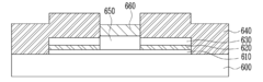
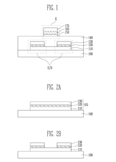
Transparent transistor and method of manufacturing the same
PatentInactiveUS20100155792A1
Innovation
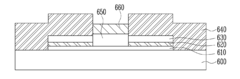
- A stacked structure for transparent transistors is implemented, comprising a substrate with source and drain electrodes having a multi-layered structure of a lower transparent layer, a metal layer, and an upper transparent layer, where the lower and upper transparent layers are formed of the same transparent semiconductor material, and a gate electrode is aligned with the channel, potentially including nitride layers for enhanced refractive index and conductivity.
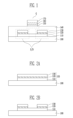
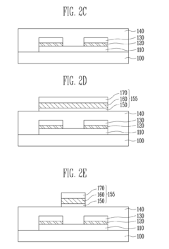
Method of manufacturing transparent transistor with multi-layered structures
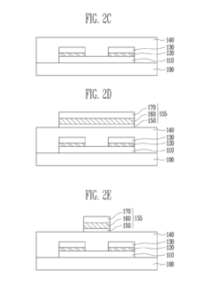
PatentInactiveUS20120315729A1
Innovation
- A stacked structure for transparent transistors is implemented, comprising a substrate with source and drain electrodes having a multi-layered structure of a lower transparent layer, a metal layer, and an upper transparent layer, where the lower and upper transparent layers are formed of the same transparent semiconductor material, and a gate electrode is aligned with the channel, potentially including nitride layers for enhanced refractive index and conductivity.
Materials Science Advancements Enabling Transparent Electronics
The evolution of transparent electronics has been fundamentally driven by breakthroughs in materials science. Traditional semiconductors like silicon, while excellent for conventional electronics, lack the optical transparency required for transparent device applications. The development of wide-bandgap oxide semiconductors has been pivotal in addressing this limitation, with materials such as indium gallium zinc oxide (IGZO), zinc oxide (ZnO), and tin oxide (SnO2) emerging as frontrunners in the field.
These oxide semiconductors offer bandgaps exceeding 3 eV, allowing visible light to pass through while maintaining semiconductor functionality. The unique electronic structure of these materials enables them to achieve electron mobilities significantly higher than amorphous silicon, while preserving optical transparency above 80% in the visible spectrum. This combination of properties was previously considered mutually exclusive in conventional semiconductor physics.
Advancements in thin-film deposition techniques have been equally crucial in the development of transparent transistor technologies. Techniques such as pulsed laser deposition (PLD), atomic layer deposition (ALD), and radio frequency magnetron sputtering have enabled the creation of high-quality oxide semiconductor films with precisely controlled thickness and composition. These methods allow for low-temperature processing, making them compatible with temperature-sensitive substrates like flexible polymers.
Doping strategies have evolved substantially to enhance the performance of transparent semiconductors. Controlled introduction of elements such as hafnium, aluminum, and nitrogen has enabled fine-tuning of carrier concentration and mobility in oxide semiconductors. Patent literature reveals significant innovation in doping methodologies that suppress oxygen vacancy formation—a common defect that causes instability in oxide-based devices.
Nanostructured materials represent another frontier in transparent electronics. Carbon-based materials like graphene and carbon nanotubes have demonstrated exceptional transparency and conductivity. Recent patents highlight novel approaches to integrating these nanomaterials with oxide semiconductors to create hybrid structures with enhanced performance characteristics.
Interface engineering has emerged as a critical focus area, with patents describing novel passivation layers and surface treatments that minimize trap states at semiconductor-dielectric interfaces. These innovations have substantially improved device stability and reduced threshold voltage shifts under prolonged operation—a persistent challenge in transparent transistor technologies.
The development of solution-processable transparent semiconductors marks a significant advancement toward cost-effective manufacturing. Patents in this domain describe novel precursor chemistries and processing methods that enable the formation of high-quality oxide semiconductor films through simple coating and annealing processes, potentially enabling roll-to-roll production of transparent electronics.
IP Landscape and Patent Strategy Considerations
The transparent transistor technology patent landscape has evolved significantly over the past two decades, with key intellectual property concentrated among several major technology companies and research institutions. Analysis of patent filings reveals that companies like Samsung, LG Display, and Sharp hold substantial patent portfolios in this domain, particularly focusing on oxide semiconductor materials such as IGZO (Indium Gallium Zinc Oxide). These patents cover fundamental material compositions, fabrication techniques, and device architectures that enable high-performance transparent electronics.
Patent activity in this field shows distinct geographical patterns, with significant concentrations in East Asia (particularly Japan, South Korea, and increasingly China), the United States, and Europe. Japanese companies initially dominated the patent landscape, but Korean and Chinese entities have rapidly increased their patent filings in recent years, indicating a shifting competitive landscape. University research institutions, particularly in the United States and Europe, continue to generate foundational patents that often become licensing opportunities for commercial entities.
Strategic patent considerations for companies entering this space must account for the dense patent thicket surrounding key materials and processes. Cross-licensing agreements have become increasingly common as no single entity possesses all necessary IP to commercialize advanced transparent transistor technologies. Patent families related to oxide semiconductor composition and deposition methods represent particularly high-value assets, as these often constitute enabling technologies with broad application potential.
Freedom-to-operate analyses reveal several potential bottlenecks where patent protection is especially strong. These include specific formulations of metal oxide semiconductors, certain thin-film deposition techniques optimized for transparent materials, and circuit design architectures that accommodate the unique electrical characteristics of transparent transistors. Companies must carefully navigate these protected areas or secure appropriate licenses.
Emerging patent trends indicate increasing focus on flexible transparent transistor technologies, environmental stability improvements, and integration methods for complex circuits. Patent applications related to manufacturing scalability and yield improvement are also gaining prominence as the technology moves toward mass production. Additionally, application-specific patents for transparent transistors in novel use cases like transparent displays, smart windows, and medical devices represent growing areas of IP development with potentially significant commercial value.
Unlock deeper insights with Patsnap Eureka Quick Research — get a full tech report to explore trends and direct your research. Try now!
Generate Your Research Report Instantly with AI Agent
Supercharge your innovation with Patsnap Eureka AI Agent Platform!