Research on Transparent Transistor Usage in Medical Devices
OCT 21, 202510 MIN READ
Generate Your Research Report Instantly with AI Agent
Patsnap Eureka helps you evaluate technical feasibility & market potential.
Transparent Transistor Technology Evolution and Objectives
Transparent transistors represent a significant technological advancement in the field of electronics, combining electrical functionality with optical transparency. The evolution of this technology can be traced back to the early 2000s when researchers first demonstrated functional transparent thin-film transistors (TTFTs) using oxide semiconductors. Prior to this breakthrough, conventional transistors relied on silicon-based materials that were inherently opaque, limiting their application in scenarios requiring visual transparency.
The development trajectory accelerated significantly around 2004 when researchers at Tokyo Institute of Technology and Oregon State University independently published groundbreaking papers on amorphous oxide semiconductors, particularly indium gallium zinc oxide (IGZO), which exhibited both high electron mobility and optical transparency. This marked a pivotal moment in transparent electronics, establishing the foundation for subsequent innovations.
Throughout the 2010s, the field witnessed substantial improvements in performance metrics, with electron mobility increasing from less than 10 cm²/Vs to over 50 cm²/Vs in optimized devices. Concurrently, manufacturing techniques evolved from laboratory-scale processes to industrial production methods, enabling the integration of transparent transistors into commercial products, primarily displays.
The medical device sector began showing interest in transparent transistor technology around 2015, recognizing its potential for creating unobtrusive, wearable health monitoring systems. The unique combination of electrical functionality and optical transparency opened new possibilities for implantable devices, smart contact lenses, and skin-attachable sensors that could continuously monitor vital signs while maintaining visual access to underlying tissues.
Current technological objectives in transparent transistor research for medical applications focus on several key areas. First, enhancing biocompatibility through the development of non-toxic, bioresorbable materials that can safely interface with human tissues. Second, improving operational stability under physiological conditions, including resistance to biofluids and temperature fluctuations. Third, reducing power consumption to enable long-term operation without frequent battery replacement or recharging.
Looking forward, the field aims to achieve fully integrated transparent medical systems that combine sensing, data processing, and wireless communication capabilities. This vision includes the development of self-powered transparent devices that can harvest energy from the human body or ambient environment, eliminating the need for external power sources and enabling truly autonomous operation.
The convergence of transparent transistor technology with advances in flexible electronics and biomedical engineering is expected to revolutionize patient monitoring and treatment delivery, potentially enabling new paradigms in personalized medicine and continuous health assessment.
Medical Device Market Demand for Transparent Electronics
The medical device market is experiencing a significant shift towards transparent electronics, driven by the increasing demand for more sophisticated, less invasive, and user-friendly healthcare solutions. Transparent electronic components, particularly transparent transistors, are becoming crucial enablers for next-generation medical devices that require both functionality and aesthetic appeal.
The global medical device market, valued at approximately $430 billion in 2020, is projected to reach $625 billion by 2027, with transparent electronics representing an emerging segment with substantial growth potential. This demand is primarily fueled by the aging population, increasing prevalence of chronic diseases, and the growing trend towards personalized healthcare and remote patient monitoring.
Wearable medical devices represent one of the most promising application areas for transparent electronics. The global wearable medical device market is expanding at a compound annual growth rate of 26.4%, with transparent components addressing key user concerns regarding comfort, discretion, and continuous wear. Devices such as smart contact lenses for glucose monitoring, transparent patch sensors for vital signs tracking, and skin-adherent electronics for drug delivery systems all benefit from the integration of transparent transistor technology.
Hospital and clinical settings are also driving demand for transparent electronics in medical imaging displays, surgical navigation systems, and augmented reality applications for medical training and procedures. The ability to overlay critical patient information onto transparent displays during surgeries or examinations without obstructing the physician's view presents a revolutionary advancement in medical visualization technology.
Point-of-care diagnostics represents another significant market segment, with transparent biosensors enabling rapid, on-site testing with improved sensitivity and specificity. The COVID-19 pandemic has accelerated this trend, highlighting the need for accessible diagnostic tools that can be deployed in various healthcare settings or even at home.
Consumer health applications, including smart mirrors with health monitoring capabilities and transparent display-integrated fitness equipment, are expanding the market beyond traditional medical settings. This consumer-facing segment is expected to grow at 18.7% annually through 2026, creating additional demand for transparent electronic components.
Regulatory considerations are shaping market demand as well, with healthcare providers increasingly seeking medical devices that comply with stringent safety standards while offering improved functionality. Transparent electronics address these needs by enabling designs that reduce infection risks through seamless surfaces and allow for better sterilization processes.
The integration of transparent electronics into implantable medical devices represents perhaps the most transformative market opportunity, with applications in neural interfaces, cardiac monitoring, and drug delivery systems that can significantly improve patient outcomes while minimizing the physical and psychological impact of having a visible medical device.
Current Limitations and Technical Barriers in Transparent Transistors
Despite the promising potential of transparent transistors in medical devices, several significant technical barriers and limitations currently impede their widespread adoption and optimal performance. The most fundamental challenge lies in achieving the delicate balance between optical transparency and electrical performance. As transparency increases, electrical conductivity and carrier mobility often decrease, creating an inherent trade-off that researchers continue to struggle with.
Material limitations represent another critical barrier. Conventional transparent conducting oxides (TCOs) like indium tin oxide (ITO) and zinc oxide (ZnO) exhibit limited flexibility, which restricts their application in wearable or implantable medical devices that require conformability to biological tissues. Additionally, these materials often demonstrate inconsistent performance under varying environmental conditions, particularly in high-humidity environments like the human body.
Fabrication challenges further complicate the integration of transparent transistors into medical devices. Current manufacturing processes typically require high-temperature annealing steps that are incompatible with temperature-sensitive medical polymers and substrates. The lack of standardized, scalable production methods results in significant device-to-device variations, hampering reliability in critical medical applications.
Stability issues present ongoing concerns for medical implementations. Transparent transistors frequently exhibit performance degradation under continuous operation, particularly when exposed to biological fluids or sterilization processes. This instability manifests as threshold voltage shifts, decreased mobility, and increased leakage currents over time, raising serious questions about long-term reliability in medical contexts.
Biocompatibility remains an underexplored area for many transparent transistor materials. While initial studies show promise, comprehensive long-term biocompatibility data is lacking for novel transparent semiconductors and dielectrics. The potential for ion leaching or degradation products in physiological environments requires thorough investigation before clinical adoption.
Interface engineering between transparent transistors and biological systems presents unique challenges. Signal transduction from biological processes to electronic signals often suffers from poor signal-to-noise ratios and limited sensitivity. Additionally, biofouling—the accumulation of proteins and cells on device surfaces—can significantly degrade sensor performance over time.
Power consumption requirements pose another limitation, particularly for implantable or wearable medical devices where battery life is critical. Current transparent transistor technologies typically exhibit higher power consumption compared to their non-transparent counterparts, necessitating trade-offs between transparency, performance, and energy efficiency.
Regulatory hurdles compound these technical challenges. The novel nature of transparent electronics in medical applications means that regulatory frameworks for their evaluation and approval remain underdeveloped, creating uncertainty in commercialization pathways and extending development timelines.
Current Implementation Methods for Transparent Transistors in Medical Devices
01 Materials for transparent transistors
Various materials can be used to create transparent transistors, including metal oxides, zinc oxide, indium oxide, and other semiconductor materials. These materials allow for the fabrication of transistors that are optically transparent while maintaining good electrical performance. The transparency enables applications in displays, touch screens, and other optoelectronic devices where visibility through the device is required.- Materials for transparent transistors: Various materials can be used to create transparent transistors, including metal oxides, zinc oxide, indium oxide, and other semiconductor materials. These materials allow for the fabrication of transistors that are optically transparent while maintaining good electrical performance. The transparency enables applications in displays, touch screens, and other optoelectronic devices where visibility through the device is required.
- Fabrication methods for transparent transistors: Different fabrication techniques are employed to create transparent transistors, including thin-film deposition, sputtering, chemical vapor deposition, and solution processing. These methods allow for the precise control of material properties and device structures. Specific processes have been developed to ensure high transparency while maintaining good electrical characteristics and stability of the transistor devices.
- Device structures and configurations: Transparent transistors can be designed in various structures including thin-film transistors (TFTs), field-effect transistors (FETs), and other novel configurations. The device architecture plays a crucial role in determining the performance characteristics such as mobility, on/off ratio, and threshold voltage. Specific structural designs can enhance transparency while optimizing electrical performance for different applications.
- Integration in display technologies: Transparent transistors are widely integrated into display technologies such as LCDs, OLEDs, and transparent displays. They serve as switching elements and pixel drivers while maintaining optical transparency. This integration enables the development of see-through displays, heads-up displays, and other advanced visualization technologies where transparency is a key requirement.
- Circuit design and performance optimization: Specialized circuit designs are developed to optimize the performance of transparent transistors in various applications. These designs address challenges related to transparency, power consumption, switching speed, and reliability. Circuit optimization techniques include novel biasing schemes, compensation methods, and layout strategies that enhance the overall performance while maintaining the transparency of the transistor-based circuits.
02 Fabrication methods for transparent transistors
Different fabrication techniques are employed to create transparent transistors, including thin-film deposition, sputtering, chemical vapor deposition, and solution processing. These methods allow for the precise control of material properties and device structures. Low-temperature processing techniques enable the use of flexible substrates, expanding the range of potential applications for transparent transistors.Expand Specific Solutions03 Device structures and architectures
Transparent transistors can be designed in various architectures, including thin-film transistors (TFTs), field-effect transistors (FETs), and vertical transistors. The device structure affects performance characteristics such as mobility, on/off ratio, and threshold voltage. Stacked or layered structures can be used to optimize both optical transparency and electrical performance, with careful consideration of the interfaces between different materials.Expand Specific Solutions04 Applications in display technology
Transparent transistors are widely used in display technologies, including liquid crystal displays (LCDs), organic light-emitting diode (OLED) displays, and electronic paper. They serve as switching elements in active-matrix displays, allowing for high-resolution, high-performance displays with improved transparency. The transparency of these transistors enables the creation of see-through displays and augmented reality devices.Expand Specific Solutions05 Circuit design and integration
Integrating transparent transistors into functional circuits requires specialized design considerations. Circuit architectures must account for the unique electrical characteristics of transparent semiconductor materials. Design tools and methodologies have been developed to optimize circuit performance while maintaining transparency. These circuits can be used in applications such as transparent logic gates, memory cells, and sensor interfaces.Expand Specific Solutions
Leading Companies and Research Institutions in Medical Transparent Electronics
The transparent transistor market for medical devices is in an early growth phase, characterized by significant research activity but limited commercial deployment. The market size is expanding as healthcare digitization accelerates, with projections suggesting substantial growth over the next decade. Technologically, transparent transistors remain in development with varying maturity levels across applications. Leading academic institutions (Oregon State University, Northwestern University, Peking University) are driving fundamental research, while commercial players demonstrate different specialization levels. Companies like LG Display and BOE Technology focus on display integration, while medical device manufacturers such as Becton Dickinson and Fresenius Medical Care are exploring implementation in healthcare products. Japanese entities including Semiconductor Energy Laboratory and Canon show advanced capabilities in specialized transparent semiconductor technologies, positioning them advantageously in this emerging field.
Oregon State University
Technical Solution: Oregon State University (OSU) has been at the forefront of transparent transistor research for medical applications since the early 2000s. Their pioneering work on amorphous oxide semiconductors, particularly zinc tin oxide (ZTO) and indium gallium zinc oxide (IGZO), has established fundamental principles for creating high-performance transparent electronic devices[1]. OSU researchers have developed transparent thin-film transistors with mobility exceeding 30 cm²/Vs while maintaining optical transparency above 85% in the visible spectrum[2]. Their innovations include low-temperature processing techniques that enable direct fabrication on biocompatible polymers for medical implants and wearables. OSU has demonstrated transparent biosensor arrays capable of detecting multiple biomarkers simultaneously while allowing visual inspection of underlying tissues. Their research extends to transparent, flexible circuits for smart bandages that can monitor wound healing parameters while permitting visual assessment without removal[3]. OSU has also pioneered the integration of transparent transistors with microfluidic systems for lab-on-chip diagnostic devices that combine electronic sensing with optical analysis capabilities. Additionally, their work on radiation-hardened transparent electronics has applications in medical imaging systems that must operate in radiation-intensive environments.
Strengths: Fundamental scientific breakthroughs in materials science and device physics that enable next-generation transparent medical electronics. Extensive intellectual property portfolio covering basic principles of transparent transistor technology. Weaknesses: As an academic institution, limited manufacturing capabilities for commercial-scale production, and potential challenges in technology transfer to industry partners.
LG Display Co., Ltd.
Technical Solution: LG Display has developed advanced transparent oxide semiconductor (TOS) technology specifically tailored for medical applications. Their proprietary metal oxide thin-film transistor (TFT) technology achieves transparency levels exceeding 85% in the visible spectrum while maintaining electrical performance comparable to conventional silicon-based transistors[1]. LG has integrated these transparent transistors into flexible, biocompatible substrates for implantable and wearable medical devices. Their technology enables the creation of transparent display panels for medical imaging that can be overlaid directly onto patients during procedures, providing surgeons with augmented reality visualization capabilities[2]. LG's transparent transistor arrays also power their innovative smart contact lens technology, which incorporates glucose sensors for continuous, non-invasive diabetes monitoring[3]. The company has further developed transparent, flexible circuits for integration into smart bandages that can monitor wound healing progress while allowing visual inspection without removal.
Strengths: Industry-leading transparency levels combined with high electrical performance. Extensive manufacturing infrastructure allows for cost-effective mass production. Weaknesses: Limited long-term biocompatibility data for implantable applications and potential challenges with hermetic sealing in biological environments.
Key Patents and Technical Breakthroughs in Transparent Transistor Design
Medical device and method of manufacturing
PatentInactiveUS7477943B2
Innovation
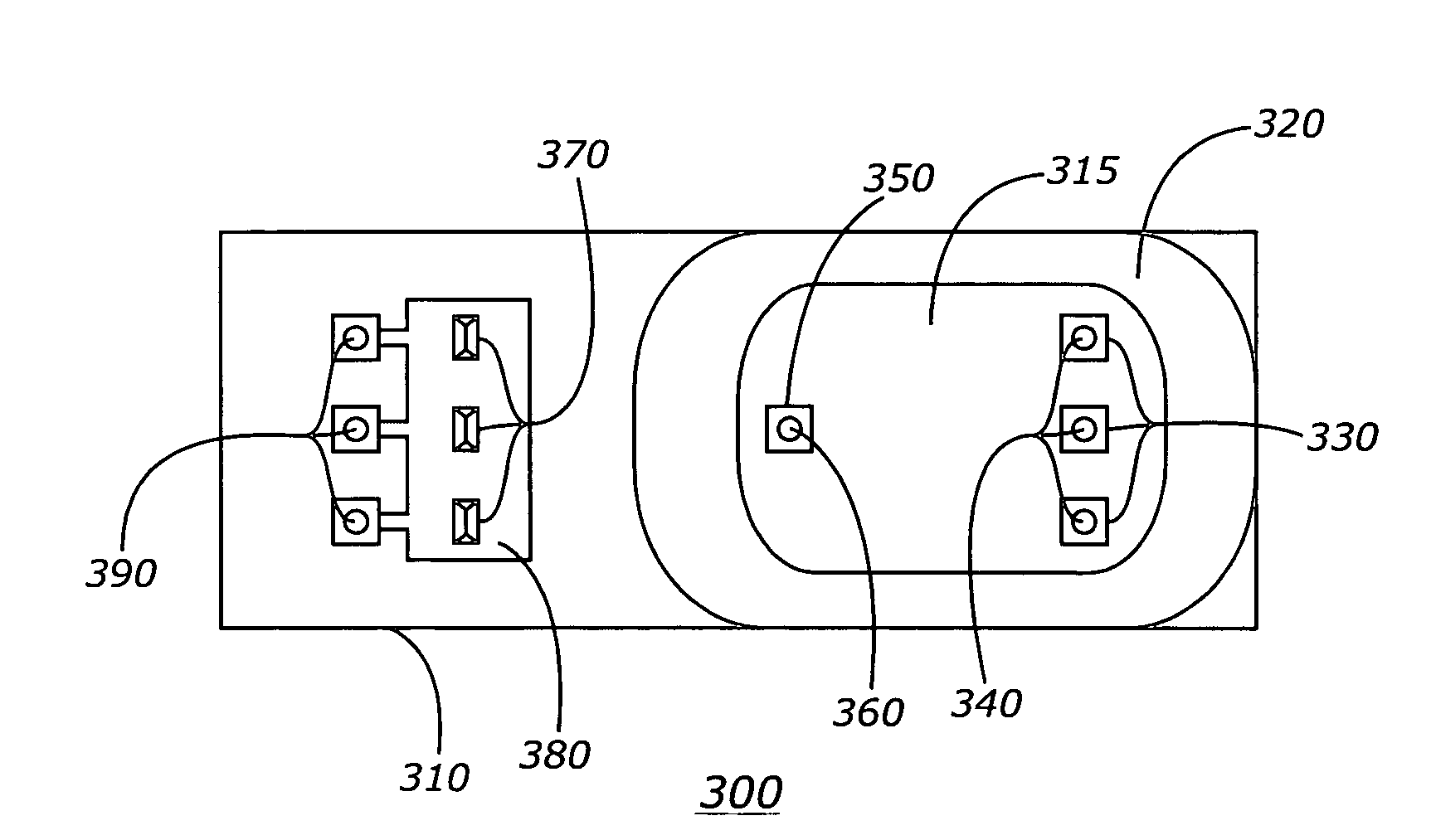
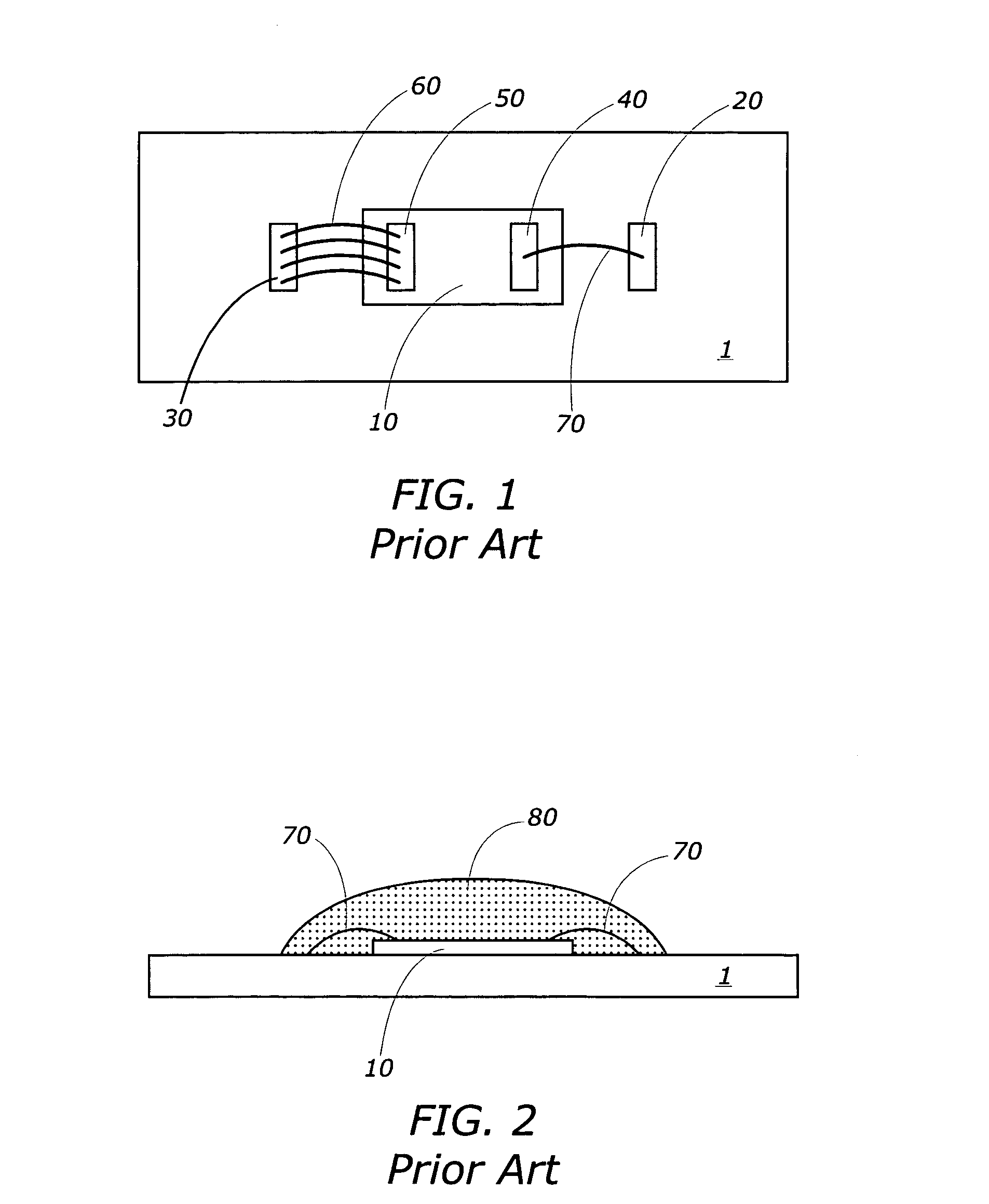
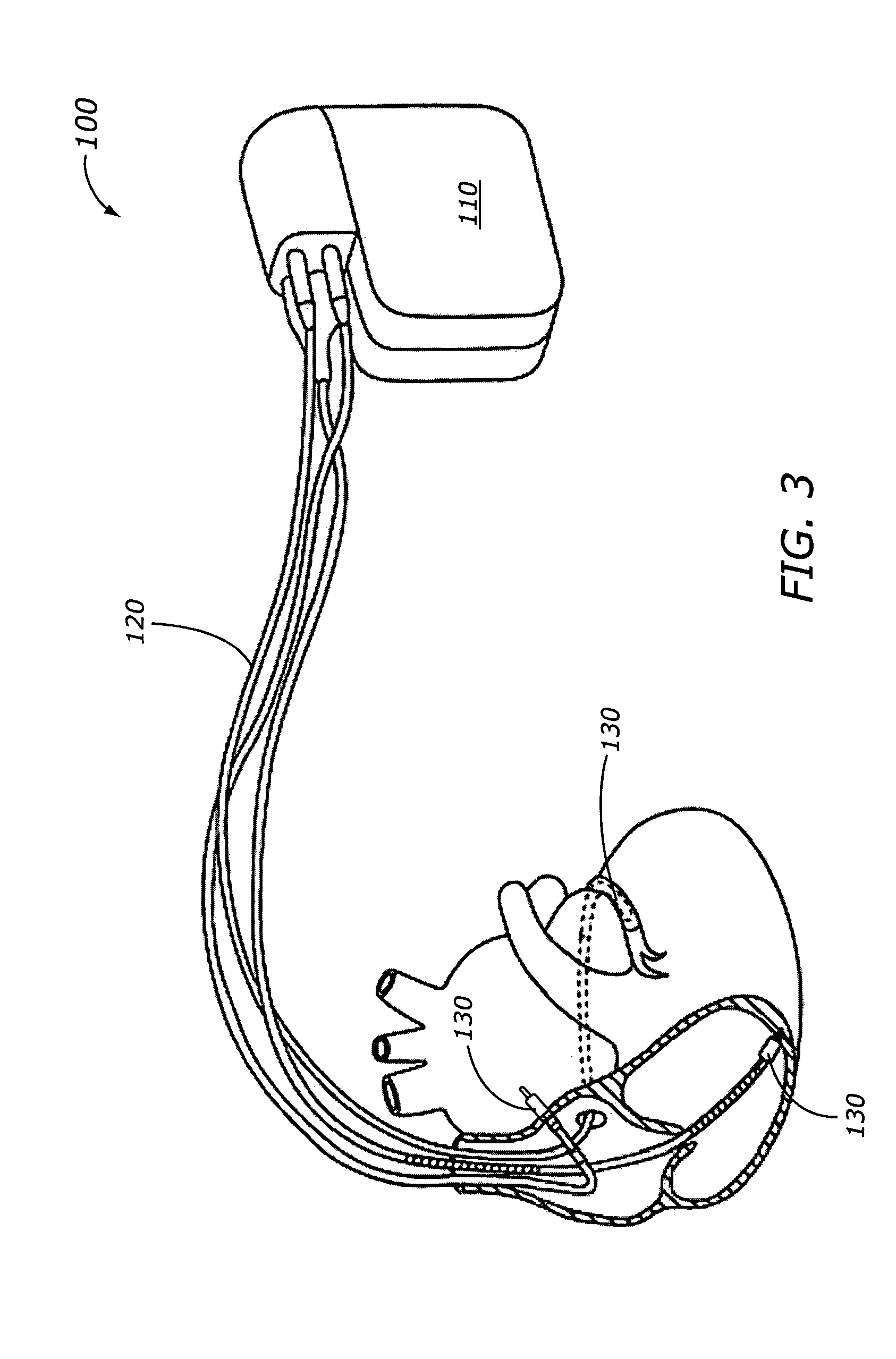
- The development of a high voltage power transistor with a semiconductor substrate and epitaxial layer, where the power transistor has vertical current flow and is mounted using a flip chip approach with solder bumps, reducing the device's footprint and increasing efficiency.
Optically transparent micromachined ultrasonic transducer (CMUT)
PatentWO2019032938A1
Innovation
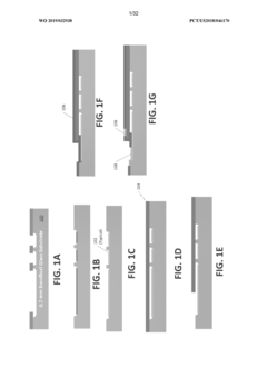
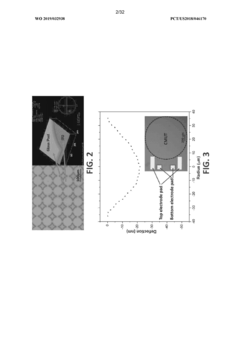
- Development of optically transparent capacitive micromachined ultrasonic transducers (CMUTs) using a glass substrate and indium-tin-oxide (ITO) electrodes, enabling improved optical transparency in the visible to near-infrared wavelength range, and employing bonding materials like BCB or SU-8 for enhanced integration with optical systems.
Biocompatibility and Safety Considerations for In-Body Applications
The integration of transparent transistors into medical implants necessitates rigorous evaluation of biocompatibility and safety parameters. Medical devices operating within the human body must meet stringent requirements to prevent adverse biological responses, including inflammation, rejection, or toxicity. Materials used in transparent transistor fabrication, such as indium gallium zinc oxide (IGZO), zinc oxide (ZnO), and various polymer substrates, require comprehensive biocompatibility testing according to ISO 10993 standards.
Cytotoxicity assessments have demonstrated that properly encapsulated transparent transistors show minimal cellular toxicity in vitro. Recent studies indicate that high-purity metal oxide semiconductors exhibit lower cytotoxicity compared to traditional silicon-based alternatives when properly isolated from direct tissue contact. However, long-term biocompatibility remains an area requiring extended clinical investigation, particularly regarding potential leaching of metal ions from the semiconductor materials.
Encapsulation technologies play a critical role in ensuring device safety. Biocompatible polymers such as parylene-C, medical-grade silicones, and polyimides have emerged as preferred encapsulation materials for transparent transistor-based implants. These materials provide effective barriers against bodily fluids while maintaining optical transparency. Multi-layer encapsulation approaches have shown superior performance in preventing ion migration and material degradation in simulated body environments.
Immune response mitigation represents another significant safety consideration. Surface modifications of transparent transistor assemblies, including anti-fouling coatings and biomimetic interfaces, have demonstrated reduced foreign body responses in preliminary animal studies. These modifications help minimize fibrous encapsulation that could otherwise compromise device functionality and optical transparency over time.
Electrical safety parameters for transparent transistor medical implants require specialized testing protocols. Operating voltages must remain within biocompatible ranges (typically below 5V) to prevent tissue damage from potential leakage currents. Researchers have developed novel circuit designs incorporating current-limiting features and redundant insulation layers to enhance safety margins for in-body applications.
Sterilization compatibility presents unique challenges for transparent transistor technologies. Common sterilization methods such as ethylene oxide, gamma radiation, and autoclave processing can potentially degrade the performance of transparent semiconductors or affect their optical properties. Recent innovations in low-temperature sterilization techniques and radiation-resistant semiconductor formulations have shown promise in addressing these limitations.
Long-term stability testing under physiological conditions remains essential for clinical translation. Accelerated aging studies simulating years of implantation have identified potential degradation mechanisms, including hydrolytic breakdown of encapsulation materials and gradual changes in transistor threshold voltages. These findings have prompted the development of more robust device architectures and predictive models for estimating in vivo performance over extended timeframes.
Regulatory Pathway for Novel Transparent Electronic Medical Devices
The regulatory landscape for transparent electronic medical devices presents unique challenges due to their novel materials and innovative applications. The FDA's regulatory framework categorizes medical devices into three classes based on risk level, with transparent transistor-based devices likely falling into Class II or III depending on their specific medical application and patient risk profile. These classifications determine the level of regulatory control and approval pathways required.
For transparent electronic medical devices, manufacturers must navigate the 510(k) clearance process or the more rigorous Premarket Approval (PMA) pathway. The 510(k) submission requires demonstrating substantial equivalence to a legally marketed predicate device, which may be challenging for novel transparent electronics without clear precedents. In such cases, the De Novo classification request provides an alternative route for low to moderate risk devices without predicates.
Clinical evaluation requirements vary significantly based on device classification and intended use. Transparent transistor-based medical devices will require comprehensive biocompatibility testing according to ISO 10993 standards, with particular attention to cytotoxicity, sensitization, and irritation potential of the transparent conductive materials. Electrical safety testing under IEC 60601 standards must address the unique properties of transparent electronics, including optical transparency maintenance during operation.
International regulatory considerations add complexity, as different regions maintain distinct approval processes. The European Union's Medical Device Regulation (MDR) employs a risk-based classification system similar to the FDA but with different technical documentation requirements. Japan's Pharmaceuticals and Medical Devices Agency (PMDA) and China's National Medical Products Administration (NMPA) have their own specific requirements for novel electronic medical devices.
Regulatory strategy development should begin early in the R&D process, incorporating pre-submission consultations with regulatory bodies to address the unique characteristics of transparent electronics. Manufacturers should establish a comprehensive quality management system compliant with ISO 13485 standards, with particular attention to risk management processes that address the novel material interfaces and optical-electronic properties.
Post-market surveillance requirements will likely be stringent for these innovative devices, requiring robust systems to monitor long-term performance, material degradation, and previously unidentified risks. Manufacturers should anticipate potential regulatory changes as transparent electronic medical device technology matures and regulatory frameworks evolve to address their unique characteristics.
Unlock deeper insights with Patsnap Eureka Quick Research — get a full tech report to explore trends and direct your research. Try now!
Generate Your Research Report Instantly with AI Agent
Supercharge your innovation with Patsnap Eureka AI Agent Platform!
