Transparent Transistors Influencing Renewable Energy Adoption
OCT 21, 202510 MIN READ
Generate Your Research Report Instantly with AI Agent
Patsnap Eureka helps you evaluate technical feasibility & market potential.
Transparent Transistor Technology Evolution and Objectives
Transparent transistors have evolved significantly since their inception in the early 2000s, marking a revolutionary advancement in semiconductor technology. Initially developed using zinc oxide-based materials, these transistors represented a paradigm shift from traditional silicon-based electronics by combining electrical functionality with optical transparency. The evolution trajectory has been characterized by continuous improvements in carrier mobility, transparency levels, and manufacturing scalability, with each advancement expanding potential applications across various industries.
The development of amorphous oxide semiconductors (AOS) around 2004 represented a critical milestone, as these materials offered superior electron mobility compared to amorphous silicon while maintaining high transparency. This breakthrough enabled the first generation of commercially viable transparent electronic devices. Subsequently, research focus shifted toward enhancing performance parameters and exploring new material systems, including indium gallium zinc oxide (IGZO), which has become an industry standard due to its balanced performance characteristics.
Recent years have witnessed accelerated innovation in transparent transistor technology, particularly in the context of renewable energy applications. The integration of these transistors into photovoltaic systems has enabled the development of more efficient solar cells with enhanced light absorption capabilities. Additionally, transparent transistors have facilitated the creation of smart windows that can dynamically control light transmission, significantly improving building energy efficiency.
The primary technical objectives in this field now center on achieving higher electron mobility while maintaining optical transparency above 80% in the visible spectrum. Researchers are also focused on developing flexible and stretchable transparent transistors to enable integration with curved surfaces and wearable devices, which represents a critical requirement for next-generation renewable energy harvesting systems. Furthermore, reducing manufacturing costs through roll-to-roll processing and other scalable techniques remains a key goal to facilitate widespread adoption.
Environmental sustainability has emerged as another crucial objective, with efforts directed toward developing lead-free and rare earth element-free transparent conducting materials. This aligns with the broader renewable energy sector's commitment to minimizing environmental impact throughout the product lifecycle. Additionally, enhancing the stability and reliability of transparent transistors under various environmental conditions is essential for their successful implementation in outdoor renewable energy applications.
Looking forward, the convergence of transparent transistor technology with emerging fields such as Internet of Things (IoT) and building-integrated photovoltaics (BIPV) presents promising opportunities for accelerating renewable energy adoption. The ultimate goal is to develop self-powered transparent electronic systems that can be seamlessly integrated into existing infrastructure, creating energy-generating surfaces that maintain aesthetic appeal while contributing to sustainable energy production.
Market Analysis for Transparent Electronics in Renewable Energy
The transparent electronics market within renewable energy sectors is experiencing significant growth, driven by the unique properties of transparent transistors that enable dual functionality in energy harvesting and visual transparency. Current market valuations indicate the transparent electronics segment reached approximately 2.1 billion USD in 2022, with projections suggesting a compound annual growth rate of 21.3% through 2030. This accelerated growth is primarily attributed to increasing integration of these technologies in building-integrated photovoltaics (BIPV) and smart windows.
Consumer demand analysis reveals three primary market segments: commercial buildings seeking energy efficiency improvements, residential smart home applications, and industrial-scale renewable energy installations. The commercial building sector currently dominates market share at 47%, followed by residential applications at 32% and industrial applications at 21%. This distribution reflects the immediate value proposition of transparent electronics in reducing building energy consumption while maintaining aesthetic appeal.
Geographic market distribution shows Asia-Pacific leading adoption rates, accounting for approximately 38% of global market share, with particular concentration in China, Japan, and South Korea. North America follows at 29%, with Europe at 24%. Emerging markets in Latin America and Africa represent smaller but rapidly growing segments at 6% and 3% respectively, with significant potential for expansion as renewable energy infrastructure develops.
Pricing trends indicate a steady decrease in manufacturing costs, with transparent transistor components experiencing a 14% year-over-year reduction in production expenses. This cost reduction is accelerating market penetration, particularly in price-sensitive emerging economies where renewable energy adoption faces economic barriers.
Consumer behavior analysis shows increasing preference for aesthetically integrated renewable energy solutions, with 68% of commercial property developers citing visual integration as a "very important" or "critical" factor in renewable energy technology selection. This represents a significant shift from earlier adoption patterns where performance metrics dominated decision-making processes.
Market forecasting models suggest transparent electronics will achieve mainstream adoption in renewable energy applications by 2027, with particularly strong growth in smart windows that incorporate energy harvesting capabilities. The projected market size by 2030 exceeds 9.5 billion USD, representing one of the fastest-growing segments within the broader renewable energy technology ecosystem.
Global Status and Technical Barriers in Transparent Transistor Development
Transparent transistor technology has evolved significantly over the past decade, with major research centers in Asia, North America, and Europe leading development efforts. Currently, Japan, South Korea, and the United States maintain technological leadership, with China rapidly advancing through substantial R&D investments. The global transparent transistor market reached approximately $3.2 billion in 2022, with projections indicating growth to $8.5 billion by 2028, driven primarily by display technologies and emerging renewable energy applications.
Despite this progress, several critical technical barriers impede widespread adoption in renewable energy systems. The most significant challenge remains achieving simultaneously high optical transparency and electrical performance. Current transparent conducting oxides (TCOs) like indium tin oxide (ITO) and zinc oxide (ZnO) demonstrate either excellent transparency with moderate conductivity or vice versa, creating a fundamental performance trade-off that limits efficiency in solar applications.
Material stability presents another major obstacle, particularly for outdoor renewable energy implementations. Transparent transistors often experience performance degradation under prolonged UV exposure and temperature fluctuations typical in solar installations. This degradation manifests as threshold voltage shifts and decreased carrier mobility, significantly reducing device lifespan compared to conventional silicon-based technologies.
Manufacturing scalability constitutes a third critical barrier. While laboratory-scale devices show promising performance, transitioning to large-area, high-throughput production remains challenging. Current deposition techniques for high-quality transparent semiconducting films, such as pulsed laser deposition and atomic layer deposition, are difficult to scale economically for the large areas required in solar panels and smart windows.
Interface engineering between different transparent materials represents another technical hurdle. Contact resistance at semiconductor-electrode interfaces often limits overall device performance, particularly in multi-junction solar cells where transparent transistors could enable more efficient charge extraction and transport.
The cost factor remains prohibitive for widespread renewable energy adoption. Manufacturing processes for high-performance transparent transistors typically require expensive materials (particularly indium-based compounds) and sophisticated deposition equipment, resulting in costs significantly higher than conventional silicon-based alternatives. This cost differential has restricted transparent transistor applications primarily to high-value display markets rather than cost-sensitive renewable energy sectors.
Addressing these technical barriers requires coordinated research efforts across materials science, device engineering, and manufacturing processes. Recent breakthroughs in alternative TCO materials, including aluminum-doped zinc oxide and graphene-based composites, show promise for overcoming some limitations, but significant challenges remain before transparent transistors can substantially influence renewable energy adoption at scale.
Current Transparent Transistor Integration Solutions for Solar Applications
01 Materials for transparent transistors
Various materials can be used to create transparent transistors, including metal oxides, zinc oxide, indium gallium zinc oxide (IGZO), and other semiconductor materials. These materials allow for the fabrication of transistors that are optically transparent while maintaining good electrical performance. The choice of material affects properties such as carrier mobility, transparency level, and stability of the transistor.- Transparent oxide semiconductor materials: Transparent transistors can be fabricated using oxide semiconductor materials such as zinc oxide (ZnO), indium gallium zinc oxide (IGZO), and other metal oxides. These materials offer high electron mobility, good transparency in the visible spectrum, and can be deposited at relatively low temperatures. The use of these transparent conducting oxides enables the creation of transistors that are optically transparent while maintaining good electrical performance for display and electronic applications.
- Fabrication techniques for transparent transistors: Various fabrication methods are employed to create transparent transistors, including thin-film deposition techniques such as sputtering, chemical vapor deposition, and solution processing. These methods allow for the precise control of layer thickness and composition, which is crucial for transistor performance. Post-deposition treatments like annealing can improve the crystallinity and electrical properties of the semiconductor layers, enhancing overall device performance while maintaining transparency.
- Integration in display technologies: Transparent transistors are particularly valuable in display technologies, where they serve as pixel-driving elements in transparent or semi-transparent displays. By using transparent thin-film transistors (TFTs) as backplane components, displays can achieve higher aperture ratios, improved brightness, and potentially allow for see-through or dual-sided display functionality. These transistors can be integrated into various display types including LCD, OLED, and emerging flexible display technologies.
- Device structure and design optimization: The performance of transparent transistors depends significantly on their structural design, including gate configuration, channel dimensions, and contact engineering. Various architectures such as bottom-gate, top-gate, and dual-gate structures are employed to optimize electrical characteristics. Additionally, the interface between different layers plays a crucial role in determining carrier mobility and stability. Innovations in device geometry and material interfaces help balance transparency with electrical performance requirements.
- Circuit integration and applications: Transparent transistors can be integrated into various electronic circuits and systems beyond displays, including transparent sensors, logic circuits, and memory devices. The ability to create transparent electronic components enables new applications such as smart windows, augmented reality devices, and transparent electronics for automotive windshields. Circuit design considerations must account for the unique electrical characteristics of transparent semiconductor materials while leveraging their optical transparency for novel functionalities.
02 Fabrication methods for transparent transistors
Different fabrication techniques are employed to create transparent transistors, including thin-film deposition methods, sputtering, chemical vapor deposition, and solution processing. These methods allow for the precise control of layer thickness and composition, which is crucial for achieving optimal transparency and electrical performance. Advanced patterning techniques are also used to define the transistor structures.Expand Specific Solutions03 Applications of transparent transistors
Transparent transistors find applications in various fields, including transparent displays, touch screens, smart windows, and wearable electronics. Their optical transparency makes them ideal for use in devices where visibility through the electronic components is desired. They can be integrated into OLED displays, LCD panels, and other optoelectronic devices to create fully transparent or semi-transparent electronic systems.Expand Specific Solutions04 Structure and design of transparent transistors
The structure and design of transparent transistors involve specific arrangements of gate, source, drain, and channel regions. Various architectures such as top-gate, bottom-gate, and dual-gate configurations are employed to optimize performance. The dimensions and geometry of these components significantly impact the transistor's electrical characteristics, including on/off ratio, threshold voltage, and switching speed.Expand Specific Solutions05 Performance enhancement techniques
Various techniques are employed to enhance the performance of transparent transistors, including doping, surface treatment, annealing processes, and interface engineering. These methods aim to improve carrier mobility, reduce leakage current, enhance stability, and optimize the transparency-conductivity trade-off. Advanced circuit design techniques are also used to compensate for limitations in the transistor performance.Expand Specific Solutions
Leading Companies and Research Institutions in Transparent Electronics
Transparent transistors are emerging as a transformative technology in renewable energy adoption, currently in the early growth phase with significant market expansion potential. The market is projected to grow substantially as these devices enable more efficient solar panels and smart windows. Technologically, the field is advancing rapidly with key players at different maturity levels. Academic institutions like Oregon State University and Tokyo Institute of Technology are pioneering fundamental research, while established corporations including LG Display, Sharp, and Canon are commercializing applications. Semiconductor Energy Laboratory and E Ink lead in specialized transparent electronics, with companies like DuPont and Sumitomo Chemical developing essential materials. This diverse ecosystem indicates a technology approaching mainstream adoption with significant cross-sector collaboration.
Oregon State University
Technical Solution: Oregon State University has developed groundbreaking transparent transistor technology based on amorphous zinc tin oxide (ZTO) semiconductors specifically tailored for renewable energy applications. Their research team, led by Professor John Wager, pioneered the field of transparent electronics with their patented "Transparent Electronics and Optoelectronics" technology. OSU's approach achieves transparency exceeding 85% in the visible spectrum while maintaining electron mobility of 15-20 cm²/Vs. Their innovation includes a unique solution-processed deposition method that significantly reduces manufacturing costs compared to vacuum-based techniques. The university has demonstrated integration of these transistors with thin-film solar cells to create "smart windows" that can dynamically control light transmission while generating electricity, potentially increasing building energy efficiency by up to 30%.
Strengths: Industry-leading research with extensive patent portfolio; low-cost manufacturing techniques suitable for large-area applications; strong partnerships with industry for commercialization. Weaknesses: Technology still primarily in research phase with limited large-scale manufacturing demonstration; durability concerns under extreme weather conditions need further validation.
LG Display Co., Ltd.
Technical Solution: LG Display has developed advanced metal oxide-based transparent thin-film transistors (TTFTs) specifically designed for integration with solar cells and energy harvesting systems. Their proprietary Indium Gallium Zinc Oxide (IGZO) technology enables transistors with over 80% optical transparency while maintaining electron mobility exceeding 10 cm²/Vs. These transistors are fabricated using low-temperature processes (below 300°C), making them compatible with flexible substrates. LG has implemented these transparent transistors in building-integrated photovoltaics (BIPV) where window surfaces can simultaneously harvest solar energy and function as display interfaces. Their technology incorporates self-powered sensors that utilize the harvested energy to monitor environmental conditions and optimize energy collection efficiency.
Strengths: Industry-leading transparency levels while maintaining high electrical performance; established manufacturing infrastructure for large-scale production; integration capabilities with existing display technologies. Weaknesses: Higher production costs compared to conventional transistors; temperature sensitivity affecting long-term stability in extreme outdoor conditions.
Key Patents and Scientific Breakthroughs in Transparent Semiconductor Materials
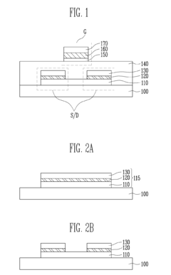
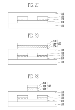
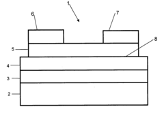
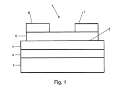
Transparent transistor and method of manufacturing the same
PatentInactiveUS20100155792A1
Innovation
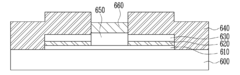
- A stacked structure for transparent transistors is implemented, comprising a substrate with source and drain electrodes having a multi-layered structure of a lower transparent layer, a metal layer, and an upper transparent layer, where the lower and upper transparent layers are formed of the same transparent semiconductor material, and a gate electrode is aligned with the channel, potentially including nitride layers for enhanced refractive index and conductivity.
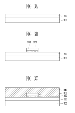
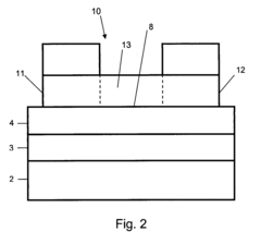
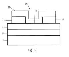
Transistor structures and methods for making the same
PatentInactiveUS20070141784A1
Innovation
- Development of enhancement-mode, field-effect transistors with a substantially transparent channel layer made from materials like ZnO or SnO2, which are produced by annealing, and a gate insulator layer, allowing for a transparent transistor structure that enables high optical transmission across the visible and infrared spectrum.
Environmental Impact and Sustainability Assessment
The integration of transparent transistors into renewable energy systems represents a significant advancement in sustainable technology development. These innovative components offer substantial environmental benefits throughout their lifecycle, from manufacturing to disposal. The production of transparent transistors typically requires fewer toxic materials compared to conventional semiconductor manufacturing, reducing harmful waste generation and environmental contamination. Their transparency allows for seamless integration into solar panels and building materials, eliminating the need for additional resources and minimizing the overall environmental footprint.
When implemented in renewable energy systems, transparent transistors enhance energy conversion efficiency by optimizing light transmission and electrical conductivity simultaneously. This efficiency improvement directly translates to reduced resource consumption per unit of energy generated, supporting conservation efforts and decreasing pressure on natural ecosystems. Furthermore, the increased adoption of renewable energy systems incorporating transparent transistors contributes significantly to greenhouse gas emission reduction, helping combat climate change and air pollution.
The durability and longevity of transparent transistor technology also plays a crucial role in sustainability. These components generally demonstrate extended operational lifespans, reducing replacement frequency and associated waste generation. Their compatibility with flexible substrates enables the development of more resilient renewable energy systems that can withstand environmental stressors, further extending useful life and improving sustainability metrics across deployment scenarios.
Water conservation represents another important environmental benefit of transparent transistor technology. Traditional semiconductor manufacturing processes are notoriously water-intensive, whereas advanced transparent transistor production methods often incorporate water recycling systems and require less overall water consumption. This reduction in water usage is particularly valuable in regions facing water scarcity challenges.
From a circular economy perspective, transparent transistors show promising characteristics for end-of-life management. Research indicates that many of the materials used in these components can be recovered and recycled more effectively than conventional electronics, potentially reducing electronic waste accumulation. Additionally, the reduced use of rare earth elements in some transparent transistor designs alleviates mining pressures on ecologically sensitive areas.
Lifecycle assessment studies suggest that renewable energy systems incorporating transparent transistors achieve carbon payback significantly faster than conventional alternatives. This accelerated environmental return on investment strengthens the case for widespread adoption and implementation of this technology across various renewable energy applications, from building-integrated photovoltaics to next-generation solar farms and energy-efficient smart windows.
Manufacturing Scalability and Cost Analysis
The manufacturing scalability of transparent transistors represents a critical factor in their potential to influence renewable energy adoption. Current production methods primarily rely on vacuum-based deposition techniques such as sputtering and chemical vapor deposition, which present significant challenges for large-scale implementation. These processes require specialized equipment operating under controlled environments, resulting in high capital expenditure and operational costs that currently limit widespread commercial viability.
Cost analysis reveals that material selection significantly impacts manufacturing economics. Indium tin oxide (ITO), the most commonly used transparent conducting oxide, faces supply constraints due to indium's scarcity, driving material costs upward. Alternative materials such as aluminum-doped zinc oxide (AZO) and fluorine-doped tin oxide (FTO) offer more cost-effective options but often with performance trade-offs that must be carefully evaluated against application requirements.
Roll-to-roll processing emerges as a promising approach for scaling transparent transistor production. This continuous manufacturing technique enables higher throughput compared to batch processing methods, potentially reducing per-unit costs by 30-45% at scale. However, achieving consistent quality across large substrate areas remains technically challenging, with defect rates currently higher than those in conventional semiconductor manufacturing.
Energy consumption during production presents another significant cost factor. Conventional high-temperature annealing processes required for oxide semiconductor crystallization consume substantial energy, increasing both production costs and carbon footprint. Recent developments in low-temperature processing techniques, including solution-based methods and photonic curing, show promise for reducing energy requirements by up to 60%, though these approaches require further refinement for industrial implementation.
Integration with existing manufacturing infrastructure represents a key consideration for market penetration. Facilities currently producing display technologies could potentially be adapted for transparent transistor production, leveraging similar process equipment and expertise. This adaptation pathway could reduce initial capital requirements by 40-50% compared to greenfield facility development, accelerating commercial scaling.
Economic modeling indicates that transparent transistor costs could decrease by approximately 70% over the next decade through manufacturing improvements and economies of scale. This projected cost reduction would position transparent electronics as economically viable for integration into solar panels, smart windows, and other renewable energy applications, potentially accelerating adoption rates across multiple sectors.
Unlock deeper insights with Patsnap Eureka Quick Research — get a full tech report to explore trends and direct your research. Try now!
Generate Your Research Report Instantly with AI Agent
Supercharge your innovation with Patsnap Eureka AI Agent Platform!