Role of Transparent Transistors in Enhancing Wearable Tech
OCT 21, 202510 MIN READ
Generate Your Research Report Instantly with AI Agent
Patsnap Eureka helps you evaluate technical feasibility & market potential.
Transparent Transistor Technology Evolution and Objectives
Transparent transistor technology has evolved significantly over the past three decades, transforming from laboratory curiosities to essential components in modern electronics. The journey began in the early 1990s with the development of the first transparent conducting oxides (TCOs), primarily focused on indium tin oxide (ITO). These materials exhibited reasonable conductivity while maintaining optical transparency, laying the groundwork for future transparent electronic devices.
By the early 2000s, researchers achieved a breakthrough with the creation of the first functional transparent thin-film transistors (TTFTs) using zinc oxide and related materials. This milestone marked the transition from passive transparent components to active transparent electronic devices capable of switching and amplification functions while maintaining visual transparency.
The evolution accelerated in the 2010s with the emergence of amorphous oxide semiconductors (AOS), particularly indium gallium zinc oxide (IGZO), which offered superior electron mobility and stability compared to earlier materials. This advancement enabled the commercial viability of transparent displays and initiated exploration into flexible transparent electronics.
Recent developments have focused on enhancing performance metrics while addressing sustainability concerns. Novel materials such as carbon-based transparent conductors (graphene, carbon nanotubes) and alternative metal oxides have emerged to reduce reliance on scarce elements like indium. Additionally, processing innovations have enabled lower temperature fabrication, making transparent transistors compatible with temperature-sensitive substrates essential for wearable applications.
The primary objective of transparent transistor technology in wearable tech is to achieve seamless integration of electronic functionality with everyday items without compromising aesthetics or user experience. This includes developing transistors with optical transparency exceeding 80% in the visible spectrum while maintaining electrical performance comparable to conventional silicon-based counterparts.
Secondary objectives include enhancing mechanical flexibility to conform to body contours, reducing power consumption to extend battery life of wearable devices, and improving environmental stability to withstand exposure to moisture, UV radiation, and temperature fluctuations encountered in daily use.
Long-term technical goals involve developing manufacturing processes compatible with roll-to-roll production to enable cost-effective mass production, creating self-powered transparent systems through integration with transparent energy harvesting technologies, and achieving biocompatibility for direct skin contact or potential implantable applications.
The convergence of these evolutionary paths and objectives positions transparent transistors as a transformative technology for wearable electronics, potentially enabling a new generation of devices that blur the distinction between technology and everyday objects, fundamentally changing how we interact with digital systems in our daily lives.
Market Demand Analysis for Transparent Wearable Electronics
The transparent wearable electronics market is experiencing unprecedented growth, driven by increasing consumer demand for seamless integration of technology into daily life. Current market research indicates that the global wearable technology market is projected to reach $265 billion by 2026, with transparent electronics representing a rapidly expanding segment within this space. This growth trajectory is supported by rising health consciousness among consumers and the expanding applications of wearable devices beyond fitness tracking to comprehensive health monitoring and augmented reality experiences.
Consumer preferences are shifting dramatically toward less obtrusive, more aesthetically pleasing wearable devices. Traditional opaque wearables are increasingly viewed as bulky and visually disruptive, creating significant market pull for transparent alternatives that can blend seamlessly with skin, clothing, or accessories. This shift is particularly pronounced in fashion-conscious demographics and professional environments where conventional wearables may be considered inappropriate or distracting.
Healthcare applications represent the most promising vertical market for transparent wearable electronics. The ability to continuously monitor vital signs through nearly invisible sensors attached directly to the skin offers revolutionary potential for chronic disease management, elderly care, and preventive medicine. Market research indicates that healthcare providers are increasingly receptive to transparent wearable solutions that improve patient compliance and data collection without disrupting normal activities.
The consumer electronics sector is also demonstrating strong demand signals, with major manufacturers investing heavily in transparent display technologies and flexible electronic components. Industry surveys reveal that approximately 72% of smartphone users express interest in complementary transparent wearable devices that extend functionality while maintaining aesthetic appeal. This represents a significant market opportunity for companies that can successfully commercialize transparent transistor technology.
Regional analysis shows varying adoption patterns, with North America and East Asia leading in both consumer demand and research investment. European markets show particular interest in sustainable and biocompatible transparent wearables, while emerging economies demonstrate rapid growth potential as manufacturing capabilities expand and prices decrease.
Supply chain analysis reveals critical bottlenecks in specialized materials production and high-precision manufacturing processes required for transparent electronics. These constraints are currently limiting market expansion and maintaining premium pricing structures. However, significant investment in manufacturing innovation suggests these barriers will diminish over the next 3-5 years, potentially triggering rapid market expansion.
The competitive landscape is evolving rapidly, with both established electronics manufacturers and specialized startups vying for market position. Strategic partnerships between materials science companies, electronics manufacturers, and fashion brands are emerging as a dominant business model, suggesting that ecosystem development will be as important as technological innovation in capturing market share.
Current Challenges in Transparent Transistor Development
Despite significant advancements in transparent transistor technology, several critical challenges continue to impede their widespread integration into wearable devices. Material limitations represent the foremost obstacle, as achieving the optimal balance between transparency and electrical performance remains difficult. Current transparent conducting oxides (TCOs) like indium tin oxide (ITO) and zinc oxide (ZnO) exhibit either insufficient carrier mobility or inadequate transparency in the visible spectrum. Additionally, these materials often demonstrate brittleness that compromises their durability in flexible wearable applications.
Manufacturing scalability presents another significant hurdle. Conventional fabrication techniques for transparent transistors typically require high-temperature processes that are incompatible with temperature-sensitive flexible substrates commonly used in wearable technology. Alternative low-temperature deposition methods often result in devices with suboptimal performance characteristics, creating a challenging trade-off between processability and functionality.
Stability issues further complicate development efforts. Transparent transistors frequently demonstrate performance degradation under environmental stressors such as humidity, temperature fluctuations, and prolonged UV exposure—conditions routinely encountered in wearable applications. This instability manifests as threshold voltage shifts, decreased carrier mobility, and increased off-state current, all of which compromise device reliability over time.
Power efficiency remains a critical concern for wearable applications where battery life is paramount. Current transparent transistor architectures typically exhibit higher operating voltages and power consumption compared to their silicon counterparts, limiting their practicality in energy-constrained wearable systems. The challenge of reducing power requirements while maintaining adequate switching speeds and signal amplification capabilities continues to challenge researchers.
Integration complexity represents another significant barrier. Incorporating transparent transistors into complete wearable systems requires compatible transparent components including conductors, capacitors, and interconnects. The heterogeneous integration of these diverse components while maintaining overall transparency and performance consistency presents formidable technical difficulties.
Standardization and testing methodologies for transparent transistors remain underdeveloped. Unlike conventional silicon-based transistors, transparent devices lack universally accepted performance metrics and testing protocols, complicating comparative analysis and quality control. This absence of standardization impedes industry-wide adoption and slows commercialization efforts.
Cost factors also present significant obstacles. Current manufacturing processes for high-performance transparent transistors involve expensive materials like indium, which faces supply constraints, and sophisticated deposition techniques that drive up production costs. These economic barriers limit commercial viability, particularly in consumer wearable markets where price sensitivity is high.
Current Implementation Methods for Transparent Transistors
01 Materials for transparent transistors
Various materials can be used to create transparent transistors, including metal oxides, zinc oxide, indium oxide, and other semiconductor materials. These materials allow for the fabrication of transistors that are optically transparent while maintaining good electrical performance. The transparency enables applications in displays, touch screens, and other optoelectronic devices where visibility through the device is required.- Transparent oxide semiconductor materials for transistors: Transparent transistors can be fabricated using oxide semiconductor materials such as zinc oxide (ZnO), indium gallium zinc oxide (IGZO), or indium tin oxide (ITO). These materials offer high optical transparency in the visible spectrum while maintaining good electrical conductivity. The use of these oxide semiconductors enables the creation of transistors that are both optically transparent and electrically functional, making them suitable for applications in transparent electronics and displays.
- Fabrication methods for transparent transistors: Various fabrication techniques are employed to create transparent transistors, including low-temperature deposition processes, solution processing, and thin-film technologies. These methods allow for the deposition of transparent semiconductor materials on glass or flexible substrates without degrading their optical or electrical properties. Advanced patterning techniques and etching processes help define the transistor structures while maintaining transparency throughout the device layers.
- Integration of transparent transistors in display technologies: Transparent transistors are increasingly being integrated into display technologies such as OLED, LCD, and transparent displays. These transistors serve as pixel-driving elements that do not block light transmission, enabling higher aperture ratios and improved display brightness. The integration allows for the development of see-through displays, heads-up displays, and augmented reality devices where visibility through the display is essential.
- Circuit design and performance optimization for transparent transistors: Specialized circuit designs are developed to optimize the performance of transparent transistors, addressing their unique electrical characteristics such as mobility limitations and threshold voltage stability. These designs include compensation circuits, novel gate structures, and optimized channel geometries. Performance optimization techniques focus on improving switching speed, reducing power consumption, and enhancing operational stability under various environmental conditions.
- Applications of transparent transistors in flexible and wearable electronics: Transparent transistors enable the development of flexible and wearable electronic devices that can conform to curved surfaces while maintaining optical transparency. These transistors are incorporated into flexible substrates to create bendable displays, transparent sensors, and wearable computing devices. The combination of transparency and flexibility opens up new possibilities for unobtrusive electronic systems that can be integrated into everyday objects, clothing, or even directly onto skin.
02 Fabrication methods for transparent transistors
Different fabrication techniques are employed to create transparent transistors, including thin-film deposition, sputtering, chemical vapor deposition, and solution processing. These methods allow for the precise control of material properties and device structures. Specific processes have been developed to ensure high transparency while maintaining electrical performance, including low-temperature processing that enables fabrication on flexible substrates.Expand Specific Solutions03 Device structures and configurations
Transparent transistors can be designed in various structures including thin-film transistors (TFTs), field-effect transistors (FETs), and other novel configurations. The device architecture plays a crucial role in determining both the optical transparency and electrical characteristics. Specific structural designs have been developed to optimize the balance between transparency and performance, including stacked layers, specialized gate configurations, and channel designs.Expand Specific Solutions04 Applications in display technology
Transparent transistors are widely used in display technologies, including LCD, OLED, and emerging display types. They serve as pixel-driving elements while maintaining optical clarity, which is essential for high-resolution displays. These transistors enable the development of transparent displays, heads-up displays, and other advanced visualization technologies where the background remains visible through the display.Expand Specific Solutions05 Circuit design and integration
Integrating transparent transistors into functional circuits requires specialized design approaches to address their unique electrical characteristics. Circuit designs must account for the specific properties of transparent semiconductor materials, including mobility, threshold voltage, and stability. Various integration techniques have been developed to incorporate transparent transistors into larger systems, including methods for connecting to conventional silicon-based electronics.Expand Specific Solutions
Leading Companies in Transparent Electronics Industry
The transparent transistor market in wearable technology is currently in an early growth phase, characterized by significant research activity and emerging commercial applications. The market size is expanding rapidly as wearable devices gain mainstream adoption, with projections indicating substantial growth over the next decade. Technologically, transparent transistors are advancing from laboratory concepts to practical implementations, with varying degrees of maturity. Leading academic institutions (Oregon State University, Northwestern University) are pioneering fundamental research, while major display manufacturers (Samsung, LG Display, BOE Technology) are commercializing applications. Japanese entities (Semiconductor Energy Laboratory, Japan Science & Technology Agency) have made significant contributions to IGZO technology, while electronics giants (HP, Motorola) are integrating these innovations into consumer products, creating a competitive landscape balanced between research institutions and commercial enterprises.
Semiconductor Energy Laboratory Co., Ltd.
Technical Solution: Semiconductor Energy Laboratory (SEL) has pioneered oxide semiconductor technology for transparent transistors, particularly focusing on IGZO (Indium Gallium Zinc Oxide) technology. Their approach involves creating highly stable amorphous oxide semiconductors that maintain excellent electron mobility (>10 cm²/Vs) while remaining optically transparent (>80% visible light transmission). SEL has developed proprietary crystallization techniques that enable consistent performance across large areas, critical for wearable displays. Their c-axis aligned crystalline IGZO technology offers superior stability under mechanical stress and bending conditions, making it particularly suitable for flexible wearable applications. SEL has also innovated in low-temperature processing methods (<300°C), enabling compatibility with temperature-sensitive substrates like polymers used in wearable tech.
Strengths: Superior electron mobility while maintaining transparency; excellent stability under mechanical stress; low-temperature processing compatibility with flexible substrates. Weaknesses: Higher manufacturing costs compared to conventional silicon; requires specialized deposition equipment; some performance degradation under extreme environmental conditions.
LG Display Co., Ltd.
Technical Solution: LG Display has developed advanced transparent transistor technology specifically optimized for wearable applications, focusing on oxide thin-film transistors (TFTs) using indium-zinc-tin oxide (IZTO) and indium-gallium-zinc oxide (IGZO) materials. Their approach integrates these transparent transistors into flexible OLED displays with ultra-thin form factors (<50 μm thickness). LG's proprietary technology enables transistors with transparency exceeding 85% in the visible spectrum while maintaining mobility values of 15-20 cm²/Vs. Their manufacturing process incorporates low-temperature deposition techniques (<200°C) compatible with flexible polymer substrates. LG has also pioneered self-aligned top-gate structures that minimize parasitic capacitance, resulting in faster switching speeds essential for responsive wearable interfaces. Their transparent transistor arrays support high pixel densities (>300 PPI) while maintaining optical clarity.
Strengths: Exceptional integration with flexible OLED technology; high transparency with good electron mobility; established mass production capabilities; optimized for low power consumption. Weaknesses: Higher cost compared to conventional display technologies; limited long-term reliability data under extreme bending conditions; requires specialized encapsulation to prevent moisture degradation.
Key Patents and Innovations in Transparent Transistor Technology
Transparent display apparatus
PatentPendingEP4580372A1
Innovation
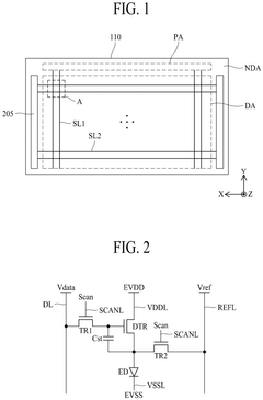
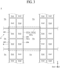
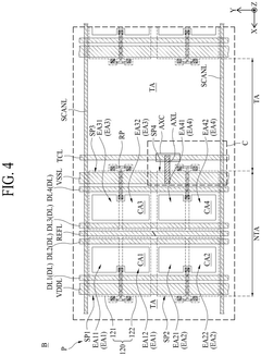
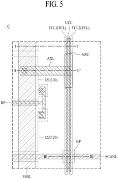
- A transparent display apparatus design featuring a substrate with a transmissive area and non-transmissive area, including power lines, trench lines, and an auxiliary power contact part to enhance light transmittance and prevent moisture ingress, allowing for a simplified structure and varied manufacturing options.
Light-emitting device and a wearable structure with light function
PatentInactiveUS20160187574A1
Innovation
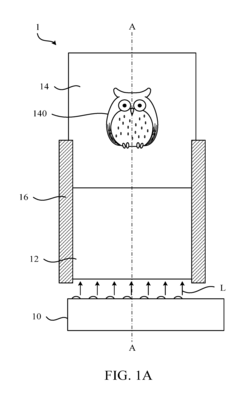
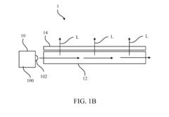
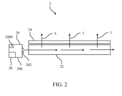
- A light-emitting device comprising a light-emitting element, a light guiding plate, and a transparent media with a removable pattern, controlled by a module that can change flashing patterns and powered by a rechargeable source, allowing users to modify visual effects by swapping transparent media without replacing the wearable structure.
Materials Science Advancements for Transparent Electronics
The evolution of transparent electronics has been fundamentally driven by breakthroughs in materials science. Traditional semiconductor materials like silicon, while excellent for conventional electronics, lack the optical transparency required for wearable technology applications. Recent advancements have focused on developing materials that combine high electrical performance with optical transparency, creating new possibilities for seamlessly integrated wearable devices.
Metal oxide semiconductors, particularly indium gallium zinc oxide (IGZO) and zinc oxide (ZnO), have emerged as leading materials for transparent transistors. These materials offer electron mobility rates significantly higher than amorphous silicon while maintaining over 80% optical transparency in the visible spectrum. The unique electronic structure of these oxides allows for efficient electron transport even in amorphous states, eliminating the need for crystalline perfection that limits traditional semiconductors.
Carbon-based nanomaterials represent another frontier in transparent electronics. Graphene, with its single-atom thickness and exceptional electrical conductivity, provides nearly perfect transparency while offering carrier mobilities exceeding 10,000 cm²/Vs at room temperature. Similarly, carbon nanotubes can be configured into transparent, flexible networks with tunable electronic properties, making them ideal for stretchable wearable applications.
Polymer-based semiconductors have also advanced considerably, with new conjugated polymers demonstrating improved charge carrier mobility while maintaining flexibility and transparency. These materials can be solution-processed at low temperatures, enabling cost-effective manufacturing on flexible substrates like polyethylene terephthalate (PET) or polyimide.
Hybrid composite materials combining inorganic semiconductors with organic polymers have shown promise in balancing performance with processability. These composites leverage the high mobility of inorganic components while benefiting from the flexibility and solution processability of organic materials, creating synergistic effects that enhance overall device performance.
Substrate engineering has progressed in parallel with semiconductor development. Ultra-thin glass (< 100 μm), flexible polyimides, and biodegradable cellulose derivatives now provide platforms that can withstand repeated bending while maintaining optical clarity. Surface treatments using atomic layer deposition have improved interface quality between these substrates and active materials, reducing defects that compromise electrical performance.
These materials science advancements collectively enable transparent transistors with performance metrics approaching those of conventional silicon devices while offering the transparency and flexibility essential for next-generation wearable technology. The continued refinement of these materials, particularly focusing on stability under mechanical stress and environmental conditions, remains crucial for widespread commercial adoption.
Energy Efficiency and Power Management in Transparent Wearables
Energy efficiency represents a critical challenge in the development of transparent wearable technologies. The integration of transparent transistors into wearable devices introduces unique power management considerations that must be addressed to ensure practical viability in real-world applications. Current transparent wearable systems typically consume between 1-10 mW/cm², significantly higher than the target consumption of <0.5 mW/cm² needed for extended operation on compact batteries.
Transparent transistors based on metal oxide semiconductors, particularly IGZO (Indium Gallium Zinc Oxide), have demonstrated promising power efficiency characteristics with static power consumption as low as 0.01 μW per transistor. However, this efficiency decreases substantially during active operation, creating a notable gap between laboratory performance and commercial requirements.
Advanced power management architectures specifically designed for transparent electronics are emerging as essential components. These systems incorporate dynamic voltage scaling, adaptive refresh rates, and context-aware operation modes that can reduce overall power consumption by 30-60% compared to conventional approaches. The implementation of transparent energy harvesting elements, such as photovoltaic cells with 10-15% transparency and 5-8% efficiency, provides supplementary power generation capabilities that extend operational lifespans.
Battery technology remains a significant bottleneck, as conventional lithium-based solutions lack transparency. Recent developments in transparent solid-state electrolytes show promise, with prototypes achieving 70% transparency while maintaining energy densities of 80-120 Wh/kg. These advances, though encouraging, still fall short of the 200+ Wh/kg densities common in opaque batteries.
Thermal management presents another critical challenge, as heat dissipation mechanisms must maintain transparency while effectively regulating device temperature. Graphene-based transparent thermal conductors have demonstrated conductivity values of 1000-2000 W/mK while maintaining 85-90% transparency, offering potential solutions for this requirement.
Industry benchmarks suggest that commercially viable transparent wearables must achieve standby times exceeding 72 hours and active usage times of 8+ hours to meet consumer expectations. Current prototypes typically achieve 40-60% of these targets, indicating substantial room for improvement. The development of specialized power management integrated circuits (PMICs) with transparency characteristics represents a promising approach to bridging this performance gap.
Unlock deeper insights with Patsnap Eureka Quick Research — get a full tech report to explore trends and direct your research. Try now!
Generate Your Research Report Instantly with AI Agent
Supercharge your innovation with Patsnap Eureka AI Agent Platform!
