Transparent Transistors for Advanced Display Technologies
OCT 21, 20259 MIN READ
Generate Your Research Report Instantly with AI Agent
Patsnap Eureka helps you evaluate technical feasibility & market potential.
Transparent Transistor Evolution and Objectives
Transparent transistors have evolved significantly since their inception in the early 2000s, transforming from laboratory curiosities to essential components in advanced display technologies. The journey began with amorphous oxide semiconductors, particularly indium gallium zinc oxide (IGZO), which offered superior electron mobility compared to traditional amorphous silicon. This breakthrough enabled the development of thinner, more energy-efficient displays with enhanced resolution and faster response times.
The evolution of transparent transistors has been driven by the increasing demand for next-generation display technologies, including flexible, foldable, and transparent displays. These applications require transistors that combine transparency with high performance, stability, and compatibility with low-temperature processing. The progression from rigid to flexible substrates has necessitated innovations in materials science and fabrication techniques to maintain electrical performance while achieving mechanical flexibility.
Recent years have witnessed the emergence of alternative materials beyond IGZO, including zinc tin oxide (ZTO), zinc oxynitride (ZnON), and two-dimensional semiconductors like graphene and MoS2. These materials offer unique advantages in terms of carrier mobility, transparency, and environmental stability. Particularly noteworthy is the development of p-type transparent semiconductors, which has opened possibilities for transparent complementary metal-oxide-semiconductor (CMOS) circuits.
The objectives of current research in transparent transistors focus on several key areas. First, enhancing electrical performance metrics, particularly carrier mobility and stability under bias stress, remains a primary goal. Second, researchers aim to develop fabrication processes compatible with large-area manufacturing at low temperatures, enabling integration with temperature-sensitive substrates. Third, achieving balanced performance in both n-type and p-type transparent transistors is crucial for realizing fully transparent integrated circuits.
Another significant objective is the integration of transparent transistors with other emerging technologies, such as organic light-emitting diodes (OLEDs) and quantum dot displays, to create novel display architectures. This integration requires careful consideration of interface engineering and compatibility between different material systems. Additionally, researchers are exploring the potential of transparent transistors beyond display applications, including transparent electronics for smart windows, augmented reality devices, and Internet of Things (IoT) sensors.
The trajectory of transparent transistor development points toward increasingly sophisticated devices that blur the line between the digital and physical worlds. As research progresses, the goal is to achieve transparent transistors with performance comparable to conventional silicon-based devices while maintaining optical transparency above 80% in the visible spectrum. This would enable truly invisible electronics that could transform how we interact with information and our environment.
Market Analysis for Advanced Display Technologies
The global market for advanced display technologies is experiencing unprecedented growth, driven by increasing consumer demand for high-quality visual experiences across multiple device categories. The transparent transistor segment represents a critical enabling technology within this ecosystem, with market projections indicating a compound annual growth rate of 21.3% between 2023 and 2028. This accelerated growth trajectory is primarily fueled by applications in transparent displays, augmented reality (AR) devices, and next-generation smart windows.
Consumer electronics continues to dominate market share, accounting for approximately 62% of transparent transistor applications. Within this sector, smartphones and tablets represent the largest sub-segment, followed by wearable devices and large-format displays. The automotive industry has emerged as the second-largest market, with heads-up displays (HUDs) and smart windshields driving adoption at a growth rate exceeding 25% annually.
Regionally, East Asia maintains market leadership with 47% of global production capacity, particularly concentrated in South Korea, Japan, and Taiwan. North America follows at 28%, with significant research activities centered in Silicon Valley and the northeastern technology corridor. Europe accounts for 18% of the market, with Germany and Finland showing particular strength in specialized applications and research.
Market analysis reveals several key demand drivers accelerating adoption. First, the miniaturization trend in consumer electronics requires increasingly transparent and efficient transistor technologies to enable higher pixel densities while maintaining optical clarity. Second, the expanding AR/VR market necessitates advanced transparent display components, with market forecasts predicting this segment will grow at 34% annually through 2027.
Industry surveys indicate that end-users prioritize three key performance metrics: optical transparency (>85%), power efficiency, and manufacturing scalability. Current market offerings average 75-80% transparency, highlighting a significant opportunity gap for technologies that can exceed this threshold while maintaining electrical performance.
Pricing trends show gradual cost reduction as manufacturing processes mature, with transparent transistor components decreasing approximately 15% in cost per unit area annually. However, this remains significantly higher than conventional transistor technologies, creating a price-performance barrier for mass-market adoption in certain applications.
The competitive landscape features both established display manufacturers and specialized startups. Major display manufacturers have invested heavily in transparent transistor R&D, with patent filings in this domain increasing by 27% annually over the past five years. Venture capital funding for startups specializing in transparent electronics has reached $1.2 billion in 2022, signaling strong investor confidence in market growth potential.
Transparent Transistor Development Status and Barriers
Transparent transistors have emerged as a critical component in advanced display technologies, with significant progress made over the past decade. Currently, several material systems dominate the landscape, including metal oxide semiconductors (particularly IGZO), organic semiconductors, and emerging 2D materials. IGZO-based transparent thin-film transistors (TFTs) have achieved commercial success in high-resolution displays due to their electron mobility exceeding 10 cm²/Vs, excellent uniformity, and compatibility with existing manufacturing infrastructure.
Despite these advancements, transparent transistor technology faces several substantial barriers. The most significant challenge remains achieving balanced performance metrics - simultaneously optimizing transparency, mobility, stability, and manufacturing scalability. Current metal oxide TFTs exhibit limited hole mobility, restricting the development of complementary circuits necessary for more energy-efficient display systems. Environmental stability presents another major obstacle, as many transparent semiconductor materials demonstrate performance degradation under prolonged exposure to ambient conditions, humidity, and light.
Manufacturing scalability constitutes a critical barrier, particularly for emerging materials like 2D semiconductors. While these materials show promising electrical properties, their integration into large-area manufacturing processes remains challenging. The industry still struggles with achieving consistent quality across large substrates while maintaining high throughput and yield rates necessary for commercial viability.
Contact resistance at semiconductor-electrode interfaces significantly limits device performance, particularly as device dimensions continue to shrink. This issue becomes more pronounced in transparent systems where conventional high-conductivity metals may compromise optical transparency. The development of transparent conductive materials with low contact resistance represents an ongoing research challenge.
From a geographical perspective, transparent transistor technology development shows distinct regional characteristics. East Asian countries, particularly Japan, South Korea, and Taiwan, lead in industrial implementation and manufacturing optimization, while North American and European research institutions focus more on fundamental materials innovation and novel device architectures. China has rapidly expanded its research capacity in this field, with significant investments in both fundamental research and manufacturing capabilities.
The performance gap between laboratory demonstrations and mass-produced devices remains substantial. While research prototypes have demonstrated impressive metrics in controlled environments, translating these achievements to production-scale devices with consistent performance, high yield, and long-term reliability continues to challenge the industry. This gap particularly affects emerging materials systems that have yet to establish mature manufacturing protocols.
Current Transparent Transistor Architectures
01 Transparent oxide semiconductor materials for transistors
Various oxide semiconductor materials can be used to create transparent transistors. These materials, such as zinc oxide (ZnO), indium gallium zinc oxide (IGZO), and other metal oxides, offer high electron mobility while maintaining optical transparency. The unique properties of these materials allow for the fabrication of transistors that can transmit visible light while still functioning as effective electronic components, making them suitable for transparent display applications.- Transparent oxide semiconductor materials for transistors: Various oxide semiconductor materials can be used to create transparent transistors. These materials, such as zinc oxide (ZnO), indium gallium zinc oxide (IGZO), and other metal oxides, offer high electron mobility while maintaining optical transparency. The unique properties of these materials allow for the fabrication of transistors that are both electrically functional and visually transparent, making them suitable for transparent display applications.
- Transparent electrode materials and structures: Transparent electrodes are crucial components in transparent transistors. Materials such as indium tin oxide (ITO), graphene, and conductive polymers can be used to create electrodes that maintain high conductivity while allowing light to pass through. The structure and deposition methods of these electrodes significantly impact the overall transparency and performance of the transistor devices.
- Transparent substrate technologies: The choice of substrate material plays a vital role in creating fully transparent transistors. Materials such as glass, flexible polymers, and transparent ceramics can serve as substrates. These materials must maintain structural integrity while offering high optical transparency. Advanced processing techniques allow for the integration of transistor components onto these transparent substrates without compromising visibility.
- Transparency enhancement techniques: Various methods can be employed to enhance the transparency of transistors. These include optimizing layer thicknesses, using anti-reflection coatings, implementing nano-structured surfaces, and developing specialized etching techniques. These approaches minimize light scattering and absorption, thereby maximizing the overall transparency of the transistor structure while maintaining electrical performance.
- Applications of transparent transistors: Transparent transistors find applications in various fields including transparent displays, smart windows, augmented reality devices, and transparent electronics. The ability to create circuits that are invisible to the human eye enables new form factors and use cases. These applications leverage the unique combination of electrical functionality and optical transparency to create innovative products that blend seamlessly with their surroundings.
02 Fabrication techniques for transparent transistor devices
Various fabrication methods are employed to create transparent transistors with optimal performance. These techniques include specialized deposition processes for transparent conductive materials, patterning methods that maintain transparency, and thermal treatments to enhance electrical properties without compromising optical clarity. Advanced manufacturing approaches help balance the competing requirements of electrical functionality and optical transparency in these devices.Expand Specific Solutions03 Integration of transparent transistors in display technologies
Transparent transistors can be integrated into various display technologies to create see-through or partially transparent screens. These transistors serve as switching elements in transparent displays while minimizing visual obstruction. The integration enables novel applications such as heads-up displays, augmented reality glasses, and transparent information displays for automotive windshields or smart windows, where maintaining visibility through the display is essential.Expand Specific Solutions04 Enhancing transparency and performance through structural design
The structural design of transparent transistors significantly impacts both their optical and electrical performance. Innovative approaches include using nanoscale materials, optimizing layer thicknesses to reduce light absorption, and developing novel device architectures that minimize opaque components. These design strategies help achieve higher transparency while maintaining or improving electrical characteristics such as on/off ratio, threshold voltage, and switching speed.Expand Specific Solutions05 Applications of transparent transistor technology
Transparent transistors enable numerous innovative applications across various industries. These include transparent electronics for smart windows that can dynamically control light transmission, flexible and transparent displays for consumer electronics, transparent sensors for unobtrusive monitoring systems, and transparent circuitry for augmented reality devices. The ability to create electronic components that don't obstruct vision opens new possibilities for integrating technology into everyday objects while maintaining their aesthetic and functional properties.Expand Specific Solutions
Industry Leaders in Transparent Transistor Manufacturing
The transparent transistor market for advanced display technologies is in a growth phase, with increasing demand driven by next-generation display applications. The competitive landscape features a mix of academic institutions (Oregon State University, MIT, Northwestern University), major display manufacturers (BOE Technology, LG Display, Samsung Display, TCL China Star), and specialized research organizations (Semiconductor Energy Laboratory, Electronics & Telecommunications Research Institute). Market competition centers around improving transparency, performance, and manufacturing scalability. Leading companies like BOE, Samsung, and LG Display are commercializing technologies, while research institutions focus on novel materials and fabrication methods. The ecosystem demonstrates global distribution across Asia (particularly Japan, China, South Korea), North America, and Europe, with increasing collaboration between academic and industrial players to accelerate technology maturation.
BOE Technology Group Co., Ltd.
Technical Solution: BOE Technology has developed advanced transparent transistor technology based on oxide semiconductor materials, primarily utilizing indium-gallium-zinc-oxide (IGZO) and zinc-tin-oxide (ZTO) compositions. Their approach features a proprietary low-temperature deposition process that enables uniform thin-film formation with controlled stoichiometry, resulting in transistors with mobility values of 15-18 cm²/Vs while maintaining optical transparency exceeding 85% in the visible spectrum. BOE's technology incorporates specialized annealing techniques that significantly reduce oxygen vacancy fluctuations, enhancing the stability of the transistors under prolonged operational conditions. Their transparent transistors feature a unique dual-gate structure that provides enhanced control over channel conductivity, resulting in improved switching performance with on/off ratios exceeding 10^8. BOE has successfully implemented these transparent transistors in commercial display products, including high-resolution LCD and OLED panels, achieving reduced power consumption and improved response times compared to conventional amorphous silicon technologies.
Strengths: Cost-effective manufacturing process compatible with existing display production lines; excellent optical transparency with good electron mobility; demonstrated reliability in mass-production environments. Weaknesses: Slightly lower mobility compared to some competitors; requires careful control of humidity during manufacturing; more sensitive to process variations affecting yield rates.
Semiconductor Energy Laboratory Co., Ltd.
Technical Solution: Semiconductor Energy Laboratory (SEL) has pioneered oxide semiconductor technology for transparent transistors, particularly focusing on IGZO (Indium Gallium Zinc Oxide) materials. Their approach involves creating highly uniform amorphous IGZO films with exceptional electron mobility (>10 cm²/Vs) while maintaining transparency above 80% in the visible spectrum. SEL has developed proprietary deposition techniques that enable precise control of oxygen vacancies in the semiconductor layer, which is crucial for stable transistor performance. Their technology incorporates unique passivation layers that protect the sensitive oxide channel from environmental degradation, resulting in devices with operational stability exceeding 10,000 hours under continuous stress conditions. SEL has successfully implemented these transparent transistors in commercial display products, achieving pixel densities exceeding 300 ppi with significantly reduced power consumption compared to conventional amorphous silicon technologies.
Strengths: Industry-leading stability and reliability in oxide semiconductor transistors; exceptional electron mobility while maintaining transparency; proven mass-production capability with established manufacturing processes. Weaknesses: Higher production costs compared to conventional technologies; requires specialized deposition equipment; more complex manufacturing process requiring precise control of oxygen content during fabrication.
Key Patents and Innovations in Transparent Semiconductors
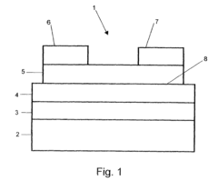
Transistor structures having a transparent channel
PatentInactiveUS7189992B2
Innovation
- Development of enhancement-mode, field-effect transistors with a substantially transparent channel layer made from materials like ZnO or SnO2, which are produced by annealing, and a gate insulator layer, allowing for a high optical transmission of at least 90% across the visible spectrum, enabling the creation of transparent thin-film transistors suitable for optoelectronic devices.
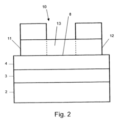
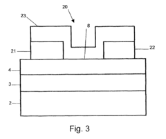
Substantially transparent display substrate, substantially transparent display apparatus, and method of fabricating substantially transparent display substrate
PatentActiveUS11563068B2
Innovation
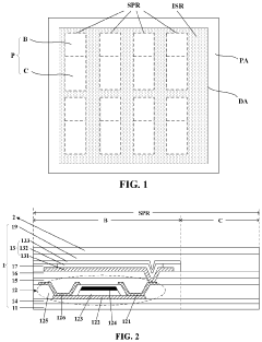
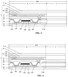
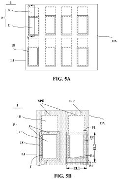
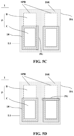
- The introduction of a substantially transparent display substrate with multiple insulating layers and strategically formed grooves in the first insulating layer, which extend into the display area and surround the edges of subpixel regions, reduces stress and allows for increased transparency by optimizing the arrangement of signal lines and layers.
Materials Science Advancements for Transparency
The evolution of transparent materials for transistor applications represents a critical frontier in display technology advancement. Traditional semiconductor materials like silicon, while offering excellent electronic properties, lack the transparency required for next-generation display technologies. Recent breakthroughs in materials science have focused on developing wide-bandgap semiconductors that combine high optical transparency with suitable electronic performance.
Metal oxide semiconductors, particularly indium gallium zinc oxide (IGZO), have emerged as leading candidates for transparent transistor applications. These materials offer optical transparency exceeding 80% in the visible spectrum while maintaining electron mobility values between 10-50 cm²/Vs. The amorphous structure of these oxides provides advantages in terms of uniformity and manufacturing scalability compared to crystalline alternatives.
Carbon-based materials represent another promising direction, with graphene demonstrating exceptional transparency (97.7% for single-layer) and theoretical electron mobility exceeding 200,000 cm²/Vs. However, challenges in bandgap engineering and large-scale production have limited its immediate commercial viability. Reduced graphene oxide (rGO) offers a more practical alternative with tunable transparency and conductivity properties.
Nanocomposite approaches combining different transparent materials have shown significant potential. Hybrid structures incorporating quantum dots within transparent oxide matrices can enhance carrier mobility while maintaining high transparency. These composites allow for engineering specific optoelectronic properties through careful material selection and structural design.
Atomic layer deposition (ALD) techniques have revolutionized the fabrication of ultra-thin transparent conductive layers with precise thickness control down to the atomic level. This enables the creation of multi-layered structures with optimized interfaces for enhanced charge transport while preserving transparency.
Solution-processing methods have advanced considerably, allowing for low-temperature deposition of transparent semiconductor materials. These approaches, including sol-gel processing and ink-jet printing, offer cost-effective alternatives to vacuum-based techniques while maintaining acceptable material quality for many applications.
The development of flexible transparent materials represents a parallel advancement track, with organic semiconductors and certain metal oxides demonstrating mechanical flexibility alongside transparency. These materials enable conformal and bendable display technologies that maintain functionality under mechanical stress, opening new application possibilities beyond conventional rigid displays.
Environmental Impact of Transparent Display Technologies
The environmental implications of transparent display technologies extend far beyond their visual appeal, encompassing the entire lifecycle from raw material extraction to end-of-life disposal. Transparent transistors, particularly those based on metal oxides like IGZO (Indium Gallium Zinc Oxide), utilize rare earth elements that pose significant extraction challenges. Mining operations for indium and gallium create substantial ecological disruptions, including habitat destruction, soil erosion, and water contamination in resource-rich regions.
Manufacturing processes for transparent displays consume considerable energy and water resources. The fabrication of high-performance transparent transistors typically requires high-temperature annealing and vacuum deposition techniques that demand intensive energy inputs. Recent life cycle assessments indicate that the production phase of transparent displays accounts for approximately 70% of their total environmental footprint, with energy consumption being the primary contributor.
Chemical usage presents another environmental concern, as the etching and cleaning processes employ hazardous substances including hydrofluoric acid and various solvents. These chemicals require stringent handling protocols and specialized waste treatment facilities to prevent environmental contamination. Emerging research into green chemistry alternatives shows promise, with water-based processing techniques potentially reducing harmful chemical usage by up to 40%.
The operational phase of transparent display technologies offers environmental benefits through reduced energy consumption. Transparent transistors enable displays with higher electron mobility and lower power requirements, potentially decreasing energy usage by 30-50% compared to conventional display technologies. This efficiency gain becomes particularly significant when considering the cumulative energy savings across millions of devices globally.
End-of-life management presents complex challenges due to the composite nature of transparent displays. The intricate integration of organic and inorganic materials complicates recycling efforts, with current recovery rates for critical elements like indium remaining below 1%. Innovative recycling technologies, including selective chemical leaching and advanced mechanical separation, are being developed to improve material recovery rates.
Recent industry initiatives have focused on designing environmentally responsible transparent display technologies. Approaches include substituting scarce materials with abundant alternatives, developing solution-processed manufacturing techniques that operate at lower temperatures, and implementing modular design principles that facilitate component replacement and eventual recycling. These developments suggest a promising trajectory toward more sustainable transparent display ecosystems.
Unlock deeper insights with Patsnap Eureka Quick Research — get a full tech report to explore trends and direct your research. Try now!
Generate Your Research Report Instantly with AI Agent
Supercharge your innovation with Patsnap Eureka AI Agent Platform!