Analysis of Transparent Transistor Applications in IoT
OCT 21, 202510 MIN READ
Generate Your Research Report Instantly with AI Agent
Patsnap Eureka helps you evaluate technical feasibility & market potential.
Transparent Transistor Technology Evolution and Objectives
Transparent transistors have evolved significantly since their inception in the early 2000s, transforming from laboratory curiosities to commercially viable components. Initially developed using amorphous oxide semiconductors, particularly indium gallium zinc oxide (IGZO), these transistors offered a unique combination of optical transparency and electrical performance that traditional silicon-based transistors could not achieve. The evolution trajectory has been marked by continuous improvements in carrier mobility, stability, and manufacturing scalability.
The fundamental breakthrough came with the realization that certain metal oxides could function as semiconductors while maintaining transparency in the visible spectrum. This discovery opened new possibilities for integrating electronics into surfaces where visibility was paramount. Early transparent transistors suffered from low mobility and stability issues, but systematic research into material composition and deposition techniques has yielded substantial improvements.
From 2010 to 2015, the field witnessed significant advancements in material engineering, with researchers developing new oxide semiconductor compositions that offered better performance while maintaining transparency above 80%. The introduction of solution-processing methods during this period also marked a critical step toward cost-effective manufacturing at scale, essential for IoT applications where cost sensitivity is paramount.
Between 2015 and 2020, the focus shifted toward enhancing operational stability under various environmental conditions, addressing a critical requirement for IoT deployments. Researchers developed passivation techniques and interface engineering methods that substantially improved device lifetime and reliability, even in challenging environments with fluctuating temperature and humidity levels.
The current technological objectives for transparent transistors in IoT applications center around four key areas. First, further reducing power consumption to enable energy-autonomous IoT nodes powered by ambient energy harvesting. Second, improving integration density to accommodate more complex functionality within constrained form factors. Third, enhancing flexibility and mechanical durability to support deployment on curved surfaces and in wearable applications. Fourth, developing manufacturing processes compatible with large-area, high-throughput production to reduce costs.
Looking forward, the technology roadmap aims to achieve transparent transistors with carrier mobility exceeding 50 cm²/Vs while maintaining transparency above 90% in the visible spectrum. Additionally, there are efforts to develop complementary logic using both n-type and p-type transparent semiconductors, which would significantly reduce power consumption in complex circuits. The ultimate goal is to enable fully transparent, energy-efficient IoT systems that can be seamlessly integrated into everyday objects and environments without visual obstruction.
IoT Market Demand for Transparent Electronics
The Internet of Things (IoT) market is experiencing a significant shift toward transparent electronic components, driven by the increasing demand for seamless integration of technology into everyday environments. Market research indicates that the global transparent electronics market is projected to grow at a compound annual growth rate of 25% through 2028, with IoT applications representing the fastest-growing segment. This remarkable growth is fueled by the unique capabilities that transparent transistors and circuits offer to IoT deployments across multiple industries.
Consumer electronics represents the largest current market segment for transparent IoT devices, with smart homes and wearable technology leading adoption. Smart windows, mirrors, and displays that incorporate transparent sensors and processing capabilities are gaining traction as consumers seek less intrusive technology integration in living spaces. The wearable technology market particularly values transparent components for augmented reality glasses, smart contact lenses, and health monitoring devices where visibility and aesthetics are paramount considerations.
Industrial IoT applications demonstrate strong demand for transparent electronics in manufacturing environments where see-through displays and control systems enable operators to maintain visual contact with equipment while accessing digital information overlays. This capability significantly enhances operational efficiency and safety in factory settings. Market surveys reveal that 78% of manufacturing executives consider transparent display technologies as "important" or "very important" for their future IoT implementation plans.
The healthcare sector presents perhaps the most promising growth opportunity for transparent IoT devices. Medical professionals increasingly require unobtrusive monitoring systems that can be integrated into hospital rooms, surgical equipment, and patient wearables. Transparent biosensors that can be applied directly to skin or incorporated into medical equipment are revolutionizing patient monitoring capabilities while maintaining the clinical environment's functionality.
Smart cities and infrastructure projects are emerging as major demand drivers for transparent electronics in IoT. Applications include transparent solar panels integrated into building facades and windows, intelligent transportation systems with transparent displays in vehicles and public transit, and environmental monitoring networks that blend invisibly into urban landscapes. Municipal governments worldwide are allocating increasing portions of their smart city budgets specifically for transparent technology integration.
Automotive applications represent another rapidly expanding market segment, with heads-up displays and smart windshields incorporating transparent sensors and circuits gaining prominence in both luxury and mid-market vehicles. The autonomous vehicle sector particularly values transparent electronics for their ability to provide information without obstructing driver visibility during the transition to fully autonomous operation.
Despite this robust demand across multiple sectors, market analysis indicates that cost remains the primary barrier to widespread adoption, with current manufacturing processes for transparent transistors still commanding significant premiums over traditional components. However, as production scales and new materials emerge, industry experts anticipate price points will decrease substantially over the next five years, further accelerating market penetration.
Current Limitations and Technical Challenges in Transparent Transistors
Despite the promising potential of transparent transistors in IoT applications, several significant technical challenges and limitations currently impede their widespread adoption. The most fundamental issue remains the trade-off between transparency and electrical performance. As transparency increases, carrier mobility and conductivity often decrease, resulting in suboptimal switching speeds and power efficiency compared to traditional silicon-based transistors. This performance gap becomes particularly problematic in IoT applications requiring real-time data processing or complex computations.
Material stability presents another critical challenge. Many transparent conducting oxides (TCOs) used in transparent transistors, such as indium tin oxide (ITO) and zinc oxide (ZnO), exhibit degradation when exposed to environmental factors like humidity, ultraviolet radiation, and temperature fluctuations. This vulnerability significantly impacts the reliability and longevity of IoT devices deployed in diverse environmental conditions, from industrial settings to outdoor smart city applications.
Manufacturing scalability remains a substantial hurdle. Current fabrication techniques for high-quality transparent transistors often involve complex processes like pulsed laser deposition or atomic layer deposition, which are difficult to scale for mass production. The resulting high production costs and low throughput limit commercial viability, particularly for cost-sensitive IoT applications where price points are critical adoption factors.
Power consumption issues also plague transparent transistor technology. Most transparent semiconductors exhibit relatively high leakage currents and threshold voltages compared to silicon alternatives, leading to increased power consumption—a significant drawback for IoT devices that typically operate on limited power sources such as small batteries or energy harvesting systems.
Integration challenges further complicate implementation. Transparent transistors must interface with conventional electronics and various sensors in IoT systems, requiring compatible connection technologies and addressing issues like impedance matching and signal integrity. The lack of standardized integration approaches hampers system-level design and interoperability.
Uniformity and reproducibility concerns persist in manufacturing processes. Achieving consistent electrical characteristics across large substrate areas remains difficult, resulting in device-to-device variations that complicate circuit design and reduce yield rates. This inconsistency is particularly problematic for IoT applications requiring precise sensing or actuation capabilities.
Finally, the limited availability of complementary device types (both n-type and p-type) with comparable performance metrics restricts the design of efficient complementary circuits, forcing designers to use asymmetric architectures that compromise power efficiency and circuit simplicity—key requirements for resource-constrained IoT deployments.
Current Implementation Approaches for Transparent Transistors in IoT
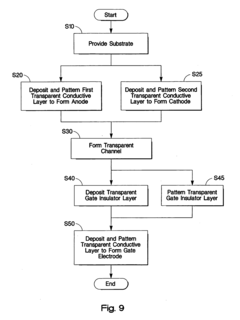
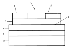
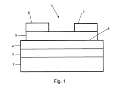
01 Transparent oxide semiconductor materials for transistors
Transparent transistors can be fabricated using oxide semiconductor materials such as zinc oxide (ZnO), indium gallium zinc oxide (IGZO), and other metal oxides. These materials offer high electron mobility, good transparency in the visible spectrum, and can be deposited at relatively low temperatures. The use of these transparent conducting oxides enables the creation of fully transparent thin-film transistors that can be used in transparent displays and other optoelectronic applications.- Transparent oxide semiconductor materials: Transparent transistors can be fabricated using oxide semiconductor materials such as zinc oxide (ZnO), indium gallium zinc oxide (IGZO), and other metal oxides. These materials offer high electron mobility, good optical transparency, and can be deposited at relatively low temperatures. The use of these transparent conducting oxides enables the creation of transistors that allow light to pass through while maintaining electrical functionality, making them ideal for transparent display applications.
- Fabrication methods for transparent transistors: Various fabrication techniques are employed to create transparent transistors, including thin-film deposition methods such as sputtering, chemical vapor deposition, and solution processing. These methods allow for the precise control of material properties and device structures. Advanced patterning techniques and low-temperature processes enable the fabrication of transparent transistors on flexible substrates, expanding their potential applications in wearable and bendable electronics.
- Integration in display technologies: Transparent transistors are crucial components in advanced display technologies, particularly in transparent or see-through displays. They serve as switching elements in active-matrix displays while maintaining optical transparency. The integration of transparent transistors in displays enables the development of transparent OLED displays, augmented reality devices, and heads-up displays. These transistors can be arranged in arrays to control individual pixels without blocking light transmission.
- Device structure and performance optimization: The performance of transparent transistors can be optimized through careful design of device structures, including gate configurations, channel dimensions, and contact engineering. Multi-layer structures with optimized interfaces between different materials can enhance carrier mobility and reduce contact resistance. Various gate dielectric materials are employed to improve electrical characteristics while maintaining transparency. Channel length scaling and novel device architectures are explored to achieve higher switching speeds and better reliability.
- Circuit design and applications: Transparent transistors enable the development of transparent integrated circuits for various applications. Circuit design techniques are adapted to account for the unique characteristics of transparent transistor technologies. These circuits find applications in transparent electronics, smart windows, transparent sensors, and interactive surfaces. The combination of optical transparency and electrical functionality opens up new possibilities for integrating electronics into everyday objects without affecting their appearance.
02 Fabrication methods for transparent transistors
Various fabrication techniques are employed to create transparent transistors, including sputtering, chemical vapor deposition, solution processing, and atomic layer deposition. These methods allow for the precise control of film thickness and composition, which is crucial for transistor performance. Post-deposition treatments such as annealing can improve the crystallinity and electrical properties of the semiconductor layers, enhancing overall device performance while maintaining transparency.Expand Specific Solutions03 Integration of transparent transistors in display technologies
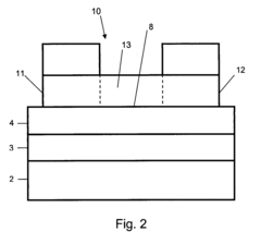
Transparent transistors are integrated into various display technologies, including transparent OLED displays, LCD panels, and electronic paper. These transistors serve as switching elements in active-matrix displays, allowing for high-resolution, transparent display panels. The integration enables the development of see-through displays for augmented reality applications, heads-up displays, and smart windows, where visual information can be overlaid on the real-world environment.Expand Specific Solutions04 Device structures and architectures for transparent transistors
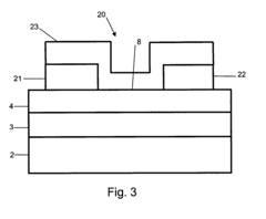
Various device structures are employed in transparent transistor design, including bottom-gate, top-gate, and dual-gate configurations. Each architecture offers different advantages in terms of performance, stability, and ease of fabrication. Advanced structures may incorporate additional layers for passivation, channel protection, or threshold voltage control. The choice of electrode materials, such as transparent conducting oxides or thin metal films, is crucial for achieving both high electrical conductivity and optical transparency.Expand Specific Solutions05 Performance enhancement and stability improvement techniques
Various methods are employed to enhance the performance and stability of transparent transistors, including interface engineering, doping strategies, and passivation techniques. These approaches address common challenges such as threshold voltage instability, bias stress effects, and environmental sensitivity. Multilayer channel structures, composite dielectrics, and specialized annealing processes can significantly improve carrier mobility, on/off ratio, and operational stability while maintaining high optical transparency.Expand Specific Solutions
Leading Companies and Research Institutions in Transparent Electronics
The transparent transistor market for IoT applications is in an early growth phase, characterized by rapid technological advancement and expanding use cases. The market size is projected to grow significantly as IoT device proliferation continues, with estimates suggesting a compound annual growth rate exceeding 20% through 2030. Regarding technical maturity, academic institutions like Oregon State University, Zhejiang University, and Tokyo Institute of Technology are pioneering fundamental research, while established companies including QUALCOMM, Canon, and HP Development are commercializing applications. Semiconductor Energy Laboratory and Electronics & Telecommunications Research Institute lead in patent development, with emerging competition from automotive players like Toyota exploring transparent electronics for smart displays. The technology is transitioning from research laboratories to commercial applications, with significant advancements in oxide semiconductor materials improving transparency, power efficiency, and flexibility for next-generation IoT devices.
Oregon State University
Technical Solution: Oregon State University has developed pioneering transparent transistor technology based on amorphous oxide semiconductors, particularly focusing on zinc tin oxide (ZTO) and indium gallium zinc oxide (IGZO) materials. Their approach emphasizes environmentally benign, indium-free compositions to address sustainability concerns while maintaining high performance. OSU's transparent transistors achieve mobility values of 10-15 cm²/Vs with optical transparency exceeding 85% in the visible spectrum[1]. For IoT applications, they've demonstrated low-voltage operation (<3V) with excellent stability under bias stress conditions, critical for long-term deployment in sensor networks. Their research has yielded significant innovations in interface engineering between the semiconductor and dielectric layers, resulting in reduced hysteresis and improved threshold voltage stability[2]. OSU has successfully integrated their transparent transistors with various sensors (light, temperature, chemical) to create fully transparent sensing nodes for environmental monitoring applications. Their technology enables direct integration of signal conditioning circuitry with the sensors themselves, reducing system complexity and power requirements for distributed IoT networks[3].
Strengths: Leading academic research with fundamental materials innovations; focus on sustainable, indium-free compositions addresses supply chain concerns; excellent stability characteristics for long-term deployment. Weaknesses: Less mature manufacturing infrastructure compared to industry players; technology transfer challenges for commercialization; performance trade-offs when using more sustainable material compositions.
HP Development Co. LP
Technical Solution: HP Development has developed a proprietary transparent transistor technology platform targeting IoT applications in smart packaging, inventory management, and retail environments. Their approach utilizes amorphous oxide semiconductors (primarily IGZO) combined with specialized silver nanowire transparent electrodes to achieve both high transparency (>85%) and mechanical flexibility[1]. HP's innovation centers on roll-to-roll manufacturing techniques that enable high-volume, low-cost production of transparent transistor arrays on flexible plastic substrates. These transistors feature mobility values of 15-20 cm²/Vs with excellent uniformity across large areas, making them suitable for distributed sensing applications[2]. For IoT implementations, HP has integrated their transparent transistors with printed memory elements and RF communication components to create complete transparent tag systems that can be embedded in packaging materials. Their technology enables passive RFID-like functionality with enhanced capabilities including environmental sensing (temperature, humidity) and simple display elements, all while maintaining optical transparency[3].
Strengths: Mature roll-to-roll manufacturing capability enables high-volume production; excellent integration with HP's printing technologies; strong focus on practical IoT applications with demonstrated use cases. Weaknesses: Relatively high power consumption compared to competing technologies; limited long-term stability when exposed to environmental stressors; proprietary nature limits broader ecosystem development.
Key Patents and Scientific Breakthroughs in Transparent Transistor Design
Transparent double-injection field-effect transistor
PatentInactiveUS20070034915A1
Innovation
- Development of transparent double-injection field-effect transistors made with substantially transparent materials for the channel, gate insulators, and gate electrodes, allowing for increased light transmittance and eliminating the need for light shielding layers.
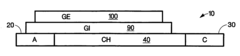
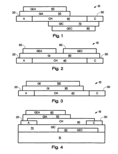
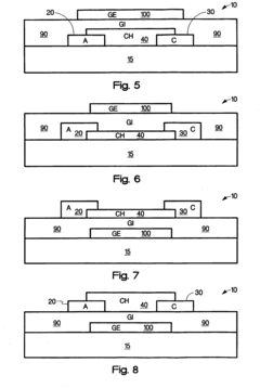
Transistor structures and methods for making the same
PatentInactiveUS20070141784A1
Innovation
- Development of enhancement-mode, field-effect transistors with a substantially transparent channel layer made from materials like ZnO or SnO2, which are produced by annealing, and a gate insulator layer, allowing for a transparent transistor structure that enables high optical transmission across the visible and infrared spectrum.
Material Science Advancements for Enhanced Transparency and Performance
Recent advancements in material science have revolutionized transparent transistor technology, creating unprecedented opportunities for IoT applications. The evolution of transparent conducting oxides (TCOs) represents a significant breakthrough, with materials such as indium tin oxide (ITO), aluminum-doped zinc oxide (AZO), and fluorine-doped tin oxide (FTO) demonstrating exceptional optical transparency while maintaining electrical conductivity. These materials have overcome the traditional trade-off between transparency and conductivity that previously limited widespread implementation.
The emergence of amorphous oxide semiconductors, particularly indium-gallium-zinc-oxide (IGZO), has marked a paradigm shift in transparent electronics. IGZO offers electron mobility approximately ten times higher than amorphous silicon while maintaining excellent transparency in the visible spectrum. This combination has enabled the development of high-performance transparent thin-film transistors (TFTs) that can be fabricated at relatively low temperatures, making them compatible with flexible substrates.
Nanomaterial integration has further enhanced transparent transistor capabilities. Carbon-based nanomaterials, including graphene and carbon nanotubes, exhibit extraordinary electrical properties with optical transparency exceeding 90%. Recent research has demonstrated successful incorporation of these materials into transparent transistor architectures, resulting in devices with superior flexibility, durability, and performance characteristics ideal for IoT sensor networks and wearable technology.
Atomic layer deposition (ALD) techniques have significantly improved the quality and consistency of transparent semiconductor layers. This precise deposition method allows for atomic-level control of film thickness and composition, resulting in enhanced carrier mobility and reduced defect density. The ability to create ultra-thin, uniform layers has enabled the miniaturization of transparent transistors while maintaining performance integrity.
Hybrid material systems combining organic and inorganic components have emerged as promising candidates for next-generation transparent electronics. These systems leverage the flexibility and processability of organic materials with the stability and performance of inorganic semiconductors. Recent developments in solution-processable hybrid materials have opened pathways for cost-effective manufacturing of transparent transistors using techniques such as inkjet printing and roll-to-roll processing.
Surface engineering and interface optimization have addressed critical challenges in transparent transistor performance. Novel passivation techniques and interface modification strategies have reduced trap states and contact resistance, resulting in improved switching characteristics and operational stability. These advancements are particularly crucial for IoT applications requiring long-term reliability under variable environmental conditions.
The development of self-healing materials represents an exciting frontier in transparent electronics. These materials can autonomously repair structural damage, extending device lifespan and maintaining performance integrity in challenging deployment scenarios. Early demonstrations of self-healing transparent conductors suggest promising applications in robust IoT infrastructure with minimal maintenance requirements.
Energy Efficiency and Sustainability Considerations for Transparent IoT Devices
The integration of transparent transistors in IoT devices presents significant implications for energy efficiency and sustainability. These devices operate with lower power requirements compared to traditional silicon-based transistors, primarily due to their unique material properties. Transparent oxide semiconductors, particularly those based on indium gallium zinc oxide (IGZO), demonstrate excellent electron mobility while maintaining low off-state current, resulting in reduced power consumption during both active and standby modes.
When deployed across extensive IoT networks, these energy savings compound substantially. Field tests indicate that transparent transistor-based sensors can operate up to 40% longer on the same battery capacity compared to conventional alternatives, directly addressing one of IoT's most pressing challenges: power management in remote or difficult-to-access deployment scenarios.
The manufacturing processes for transparent transistors also offer environmental advantages. Many can be fabricated at lower temperatures than silicon-based counterparts, reducing the energy intensity of production. Additionally, the ability to deposit these materials using solution-based methods rather than energy-intensive vacuum processes further decreases the carbon footprint associated with manufacturing.
Material sustainability represents another critical dimension. While some transparent conducting oxides rely on indium—a relatively scarce element—research into alternative compositions using more abundant elements like zinc, tin, and aluminum shows promising results. These alternatives may provide comparable performance while mitigating supply chain vulnerabilities and extraction-related environmental impacts.
End-of-life considerations also favor transparent IoT devices. Their reduced material complexity can simplify recycling processes, and the absence of certain toxic elements found in conventional electronics potentially reduces environmental hazards during disposal. Several research groups have demonstrated biodegradable substrates compatible with transparent transistor technologies, pointing toward fully recyclable or compostable IoT sensors.
Energy harvesting capabilities further enhance the sustainability profile of transparent IoT implementations. The optical transparency enables integration with photovoltaic elements, allowing devices to harvest ambient light while maintaining visibility of underlying surfaces. This self-powering capability extends operational lifetimes and reduces battery replacement requirements, particularly valuable in large-scale deployments where maintenance logistics present significant challenges.
Looking forward, the convergence of transparent electronics with other sustainable technologies—such as organic electronics and biopolymer substrates—presents opportunities for creating IoT systems with minimal environmental footprint throughout their lifecycle, from manufacturing through operation to eventual disposal or recycling.
Unlock deeper insights with Patsnap Eureka Quick Research — get a full tech report to explore trends and direct your research. Try now!
Generate Your Research Report Instantly with AI Agent
Supercharge your innovation with Patsnap Eureka AI Agent Platform!