Transparent Transistor Market Forecast: A Strategic Analysis
OCT 21, 20259 MIN READ
Generate Your Research Report Instantly with AI Agent
Patsnap Eureka helps you evaluate technical feasibility & market potential.
Transparent Transistor Evolution and Objectives
Transparent transistors have evolved significantly since their inception in the early 2000s, marking a revolutionary advancement in display and electronics technology. Initially developed using amorphous oxide semiconductors, particularly indium gallium zinc oxide (IGZO), these transistors offered unprecedented combinations of optical transparency and electrical performance. The evolution trajectory has been characterized by continuous improvements in carrier mobility, stability, and manufacturing scalability, transitioning from laboratory curiosities to commercial viability within two decades.
The fundamental technological breakthrough enabling transparent transistors was the development of wide-bandgap semiconductor materials that could simultaneously conduct electricity while remaining visually transparent. Early iterations faced significant challenges including low electron mobility, instability under environmental stressors, and manufacturing complexity. However, systematic research efforts have progressively addressed these limitations, resulting in today's high-performance transparent thin-film transistors (TTFTs).
Current technological objectives in the transparent transistor domain focus on several critical dimensions. First, enhancing electrical performance metrics, particularly carrier mobility exceeding 50 cm²/Vs while maintaining transparency above 80% in the visible spectrum. Second, improving operational stability under prolonged use and environmental exposure, targeting operational lifetimes exceeding 10,000 hours under standard conditions. Third, developing manufacturing processes compatible with large-area, low-temperature deposition to enable integration with flexible substrates.
The industry is witnessing a convergence of research efforts toward solution-processable oxide semiconductors, which promise dramatic reductions in manufacturing costs while maintaining performance comparable to vacuum-deposited counterparts. Zinc tin oxide (ZTO) and aluminum-doped zinc oxide (AZO) have emerged as promising alternatives to traditional IGZO, offering reduced reliance on scarce indium resources.
Looking forward, the technological roadmap for transparent transistors encompasses several ambitious objectives. These include achieving ultra-high mobility (>100 cm²/Vs) transparent semiconductors, developing fully transparent and flexible integrated circuits, and enabling low-power operation for mobile and IoT applications. Additionally, there is growing interest in developing p-type transparent semiconductors to complement existing n-type materials, potentially enabling transparent CMOS technology.
The evolution of transparent transistors is increasingly influenced by sustainability considerations, with research efforts directed toward earth-abundant materials and environmentally friendly processing methods. This aligns with broader industry trends toward green electronics and circular economy principles, positioning transparent transistor technology not only as an enabler of next-generation displays but also as a component of sustainable electronic ecosystems.
Market Demand Analysis for Transparent Electronics
The transparent electronics market is experiencing unprecedented growth driven by increasing demand for innovative display technologies and smart devices. Current market analysis indicates that the global transparent electronics sector is valued at approximately $3.2 billion as of 2023, with projections suggesting expansion to reach $7.5 billion by 2030, representing a compound annual growth rate of 12.8% during the forecast period.
Consumer electronics remains the dominant application segment, accounting for nearly 45% of market share. This is primarily fueled by the rising adoption of transparent displays in smartphones, tablets, and wearable devices. The automotive industry represents the second-largest market segment at 22%, where transparent electronics are increasingly integrated into heads-up displays, smart windshields, and interactive dashboard systems.
Regionally, Asia-Pacific leads the market with approximately 38% share, driven by the strong presence of electronics manufacturing hubs in countries like South Korea, Japan, Taiwan, and China. North America follows at 29%, with Europe accounting for 24% of the global market. Emerging economies in Latin America and Africa are showing promising growth potential, albeit from a smaller base.
The demand for transparent electronics is significantly influenced by several key factors. Energy efficiency requirements are paramount, as consumers and regulatory bodies increasingly prioritize sustainable technologies. This has accelerated research into low-power transparent transistors and circuits. Additionally, the growing smart home market, valued at $112 billion in 2023, is creating substantial demand for transparent interfaces and control systems.
Healthcare applications represent one of the fastest-growing segments, with transparent biosensors and monitoring devices gaining traction. The medical transparent electronics sub-segment is expected to grow at 15.7% annually through 2030, outpacing the overall market average.
Consumer preference surveys indicate strong interest in transparent display technologies, with 67% of respondents expressing willingness to pay premium prices for devices incorporating transparent screens. This consumer sentiment is particularly strong among younger demographics (18-34 years), where the preference rate increases to 78%.
Industry analysts predict that the integration of transparent electronics with emerging technologies like 5G, Internet of Things (IoT), and artificial intelligence will create new market opportunities. The smart city infrastructure segment, for instance, is expected to grow at 14.2% annually, creating demand for transparent electronic signage, interactive kiosks, and smart windows.
Technical Barriers and Global Development Status
Despite significant advancements in transparent transistor technology, several technical barriers continue to impede widespread commercial adoption. The primary challenge remains achieving the optimal balance between transparency and electrical performance. Current transparent conducting oxide (TCO) materials like indium tin oxide (ITO) and zinc oxide (ZnO) face limitations in carrier mobility, which directly impacts switching speed and power efficiency. Additionally, the stability of these materials under various environmental conditions presents ongoing reliability concerns.
Manufacturing scalability represents another significant hurdle. While laboratory demonstrations have shown promising results, transitioning to mass production while maintaining consistent performance parameters across large substrate areas remains problematic. The precision required for uniform thin-film deposition at industrial scales introduces yield challenges that affect production economics.
Globally, development status varies significantly by region. East Asia, particularly Japan, South Korea, and Taiwan, leads in transparent transistor research and commercialization efforts. These regions benefit from established display manufacturing ecosystems and substantial government investment in next-generation electronics. Companies like Samsung, LG Display, and Sharp have made notable progress in integrating transparent transistor technology into prototype display products.
North America maintains strong positions in fundamental research through university and corporate R&D centers, with companies like Apple and Google exploring applications in augmented reality devices. The European landscape features specialized research clusters focused on novel materials and sustainable manufacturing processes, with particular strength in organic and hybrid transparent semiconductor development.
Emerging economies, especially China, have rapidly accelerated their development efforts, with significant investments in manufacturing infrastructure and intellectual property acquisition. Chinese companies have increasingly shifted from being manufacturing partners to innovation leaders, particularly in consumer electronics applications of transparent transistors.
The technical maturity of transparent transistor technology varies by application domain. Display applications have reached higher technology readiness levels, while emerging applications in smart windows, transparent electronics, and wearable devices remain at earlier development stages. This uneven development reflects both market priorities and the varying technical requirements across applications.
Standardization efforts remain fragmented, with multiple competing technical approaches and limited industry consensus on performance metrics and testing protocols. This fragmentation complicates supply chain development and slows broader ecosystem formation around transparent transistor technology.
Current Technical Solutions and Implementation
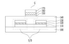
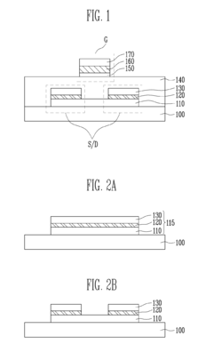
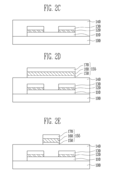
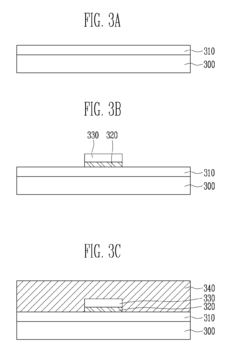
01 Transparent oxide semiconductor materials for transistors
Transparent transistors can be fabricated using oxide semiconductor materials such as zinc oxide (ZnO), indium gallium zinc oxide (IGZO), and other metal oxides. These materials offer high electron mobility, good transparency in the visible spectrum, and can be deposited at relatively low temperatures. The use of these oxide semiconductors enables the creation of transistors that are both electrically functional and optically transparent, making them suitable for display applications and transparent electronics.- Materials for transparent transistors: Various materials can be used to create transparent transistors, including metal oxides, zinc oxide, indium oxide, and other semiconductor materials. These materials allow for the fabrication of transistors that are optically transparent while maintaining electrical functionality. The choice of material affects properties such as carrier mobility, transparency level, and overall performance of the transistor. Transparent conducting oxides (TCOs) are particularly important in this field as they combine electrical conductivity with optical transparency.
- Fabrication methods for transparent transistors: Various fabrication techniques are employed to create transparent transistors, including thin-film deposition methods, sputtering, chemical vapor deposition, and solution processing. These methods allow for the precise control of layer thickness and composition, which is crucial for transistor performance. Low-temperature processing techniques enable the use of flexible substrates, expanding the application range of transparent transistors. The fabrication process often involves multiple steps including substrate preparation, deposition of active layers, patterning, and electrode formation.
- Applications of transparent transistors in display technology: Transparent transistors are widely used in display technologies such as transparent displays, OLED displays, and LCD panels. They enable the creation of fully transparent or see-through display devices by eliminating opaque components traditionally used in display backplanes. These transistors can be integrated into active-matrix displays to control individual pixels while maintaining optical clarity. The transparency allows for innovative display designs including heads-up displays, augmented reality devices, and transparent electronic signage.
- Structure and design of transparent transistors: The structure of transparent transistors typically includes a transparent substrate, transparent conducting electrodes, a transparent semiconductor layer, and insulating layers. Various designs such as top-gate, bottom-gate, and dual-gate configurations are used depending on the specific application requirements. The transistor architecture affects parameters such as on/off ratio, threshold voltage, and switching speed. Advanced designs may incorporate multiple channels, heterojunctions, or novel gate structures to enhance performance while maintaining transparency.
- Performance enhancement and optimization techniques: Various techniques are employed to enhance the performance of transparent transistors, including doping, surface treatment, interface engineering, and annealing processes. These methods aim to improve carrier mobility, reduce threshold voltage, enhance stability, and increase transparency. Optimization of layer thicknesses and compositions can significantly impact transistor performance. Advanced techniques such as atomic layer deposition and high-k dielectric integration are used to achieve better electrical characteristics while maintaining optical transparency.
02 Fabrication methods for transparent transistors
Various fabrication techniques are employed to create transparent transistors, including thin-film deposition methods such as sputtering, chemical vapor deposition, and solution processing. These methods allow for the precise control of layer thickness and composition. Post-deposition treatments like annealing can improve the crystallinity and electrical properties of the semiconductor layers. Advanced patterning techniques ensure accurate definition of transistor structures while maintaining transparency across the device.Expand Specific Solutions03 Integration of transparent transistors in display technologies
Transparent transistors are crucial components in advanced display technologies, particularly in transparent or see-through displays. They serve as pixel-driving elements that do not block light transmission through the display panel. The integration of these transistors enables the development of heads-up displays, augmented reality devices, and transparent OLED or LCD panels. Their implementation allows for novel display architectures where the active matrix backplane does not impede visibility.Expand Specific Solutions04 Electrode and dielectric materials for transparent transistors
The development of suitable electrode and dielectric materials is essential for transparent transistor performance. Transparent conductive oxides like indium tin oxide (ITO) and aluminum-doped zinc oxide (AZO) are commonly used as electrode materials. High-quality transparent dielectric materials such as aluminum oxide, silicon dioxide, and hafnium oxide provide effective gate insulation while maintaining optical transparency. The selection and optimization of these materials significantly impact the transistor's electrical characteristics and overall transparency.Expand Specific Solutions05 Performance optimization and circuit design for transparent transistors
Enhancing the performance of transparent transistors involves optimizing carrier mobility, on/off current ratio, threshold voltage stability, and reducing leakage currents. Circuit design considerations include addressing the unique electrical characteristics of transparent transistors when integrating them into larger systems. Specialized layout techniques and compensation circuits may be employed to overcome limitations in switching speed or current driving capability. These optimizations enable transparent transistors to meet the requirements of various applications while maintaining their optical transparency.Expand Specific Solutions
Key Industry Players and Competitive Landscape
The transparent transistor market is currently in a growth phase, characterized by increasing adoption across display technologies and emerging applications. The market size is expanding rapidly, driven by demand for transparent electronics in consumer devices, automotive displays, and smart windows. Technologically, the field is advancing from early-stage development toward commercial maturity, with key players demonstrating different levels of innovation. Academic institutions like Oregon State University, Zhejiang University, and Tokyo Institute of Technology are pioneering fundamental research, while commercial entities including BOE Technology, LG Display, and Japan Display are focusing on manufacturing scalability. Companies such as Samsung Mobile Display and Canon are advancing integration capabilities, while specialized firms like Semiconductor Energy Laboratory and Advanced Nano Products are developing novel materials and fabrication techniques essential for next-generation transparent transistor technologies.
BOE Technology Group Co., Ltd.
Technical Solution: BOE has developed advanced metal oxide semiconductor (AMOX) transparent transistor technology for their display products. Their solution incorporates indium gallium zinc oxide (IGZO) transistors with high electron mobility (>10 cm²/Vs) and transparency exceeding 90% in the visible spectrum. BOE's transparent transistor technology enables the production of borderless displays with integrated touch functionality and improved optical performance. The company has implemented this technology in their flexible OLED displays and transparent display products, achieving pixel densities above 400 PPI while maintaining high transparency. BOE has also developed proprietary manufacturing processes that allow for low-temperature deposition of transparent transistor materials, enabling compatibility with flexible substrates and reducing production costs compared to traditional silicon-based approaches.
Strengths: Industry-leading production capacity for transparent displays; vertical integration from materials to finished products; strong R&D capabilities with over 1,000 patents in transparent electronics. Weaknesses: Relatively higher manufacturing costs compared to conventional technologies; challenges in achieving uniform electrical properties across large-area substrates.
LG Display Co., Ltd.
Technical Solution: LG Display has pioneered transparent transistor technology based on amorphous oxide semiconductors, particularly focusing on indium-gallium-zinc-oxide (IGZO) and indium-tin-zinc-oxide (ITZO) materials. Their transparent transistor solution achieves mobility values of 15-20 cm²/Vs while maintaining optical transparency above 85%. LG has integrated these transistors into their transparent OLED and LCD display products, enabling applications in automotive heads-up displays, retail showcases, and smart home appliances. The company has developed a proprietary "invisible electrode" technology that reduces the visibility of circuit patterns in transparent displays by using ultra-thin metal oxide conductors with optimized optical properties. LG's manufacturing approach employs low-temperature sputtering processes that allow for uniform deposition across large substrates (Gen 8.5 and above), supporting mass production of transparent display products.
Strengths: Extensive experience in mass production of transparent displays; strong vertical integration from materials to finished products; advanced manufacturing facilities optimized for oxide semiconductor processing. Weaknesses: Higher cost structure compared to conventional display technologies; challenges in achieving consistent electrical performance under varying environmental conditions.
Core Patents and Technical Literature Review
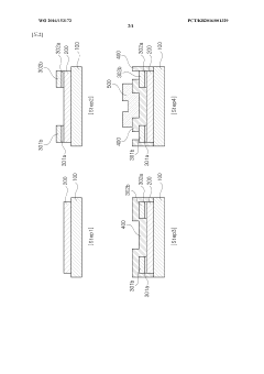
Transparent transistor with multi-layered structures and method of manufacturing the same
PatentInactiveUS8269220B2
Innovation
- A stacked structure for transparent transistors is implemented, comprising a substrate with source and drain electrodes having a multi-layered structure of a lower transparent layer, a metal layer, and an upper transparent layer, where the lower and upper transparent layers are formed of the same transparent semiconductor material, and a gate electrode is aligned with the channel, potentially including nitride layers for improved refractive index and conductivity.
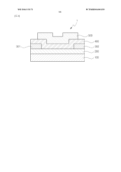
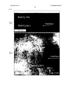
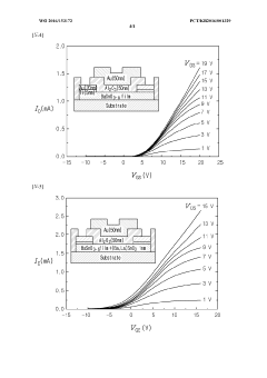
Basno3 thin film transistor having high field-effect mobility, and manufacturing method therefor
PatentWO2016153172A1
Innovation
- Development of barium stannate (BaSnO3) thin film transistors with oxygen-deficient or impurity-injected n-type semiconductor oxide thin films, deposited in the c-axis direction on suitable substrates, using techniques like pulse laser deposition or sputtering, to achieve high field-effect mobility and thermal stability.
Supply Chain Analysis and Material Dependencies
The transparent transistor supply chain exhibits a complex structure with multiple critical dependencies that significantly impact market dynamics. Raw material sourcing represents the foundation of this ecosystem, with indium, gallium, zinc, and tin serving as essential elements for transparent conducting oxides (TCOs). Indium tin oxide (ITO) remains the dominant material despite supply constraints, with indium primarily sourced from China (approximately 55% of global production), South Korea, and Japan. This geographic concentration creates inherent supply vulnerabilities that manufacturers must navigate through strategic partnerships and inventory management.
Material processing capabilities present another critical dependency, requiring specialized equipment for thin-film deposition techniques such as sputtering, chemical vapor deposition, and atomic layer deposition. The precision equipment market is dominated by established players from Japan, Germany, and the United States, creating potential bottlenecks during periods of high demand. Notably, the semiconductor equipment manufacturers have begun expanding their offerings to address the growing transparent electronics sector.
Component integration represents a mid-chain vulnerability point where specialized manufacturing expertise becomes essential. The ability to integrate transparent transistors with other electronic components while maintaining optical transparency requires advanced manufacturing processes primarily concentrated in East Asia. Taiwan, South Korea, and Japan collectively control approximately 70% of this integration capability, creating regional dependencies that impact global production capacity.
Quality control systems throughout the supply chain introduce additional complexity, as transparent transistors require stringent performance parameters including optical transparency exceeding 80%, consistent electrical conductivity, and mechanical flexibility. The specialized testing equipment necessary for these quality assurance processes is predominantly supplied by European and American firms, creating another potential constraint point during market expansion phases.
Logistics and distribution networks complete the supply chain picture, with finished transparent transistor components requiring specialized handling and environmental controls during transport. The COVID-19 pandemic exposed vulnerabilities in this aspect of the supply chain, with manufacturers now implementing redundancy strategies including regional manufacturing hubs and diversified shipping partnerships to mitigate future disruptions.
Material recycling and sustainability initiatives are emerging as important considerations within the supply chain, particularly given the limited global reserves of indium and other critical materials. Several leading manufacturers have initiated closed-loop recycling programs, though recovery rates remain below 35% industry-wide, presenting both a challenge and opportunity for supply chain optimization as the market continues its projected growth trajectory.
Sustainability and Environmental Impact Assessment
The environmental impact of transparent transistor technology represents a critical dimension in market development that cannot be overlooked. Transparent transistors, primarily based on metal oxide semiconductors like IGZO (Indium Gallium Zinc Oxide), offer significant sustainability advantages compared to conventional silicon-based technologies. These devices typically require lower processing temperatures, reducing energy consumption during manufacturing by approximately 30-40% compared to traditional transistor production methods.
Material sourcing presents both challenges and opportunities for sustainable development in this sector. The reliance on rare elements such as indium raises concerns about resource depletion and extraction impacts. Current estimates suggest that indium reserves may face constraints within 20-30 years at projected consumption rates. However, research into alternative materials such as zinc tin oxide (ZTO) demonstrates promising potential for reducing dependence on scarce resources while maintaining performance characteristics.
End-of-life considerations for transparent electronics reveal favorable recyclability profiles. The thin-film nature of these devices allows for more efficient material recovery compared to conventional electronics. Studies indicate that up to 85% of the metal oxide components can be reclaimed through appropriate recycling processes, significantly reducing waste generation and supporting circular economy principles.
Energy efficiency during operation represents another substantial environmental benefit. Transparent transistors typically consume 40-60% less power than their silicon counterparts in comparable applications, translating to reduced carbon footprints across product lifecycles. This efficiency gain becomes particularly significant in always-on display technologies and IoT applications where power consumption is a critical factor.
Manufacturing processes for transparent transistors are evolving toward greater environmental responsibility. Solution-based deposition methods are replacing vacuum-based techniques, reducing chemical waste by up to 70% and decreasing water usage in production facilities. Several leading manufacturers have committed to carbon-neutral production by 2030, implementing renewable energy sources and closed-loop water systems in new fabrication plants.
Regulatory frameworks increasingly influence market dynamics, with the EU's Restriction of Hazardous Substances (RoHS) and Registration, Evaluation, Authorization and Restriction of Chemicals (REACH) regulations imposing strict guidelines on material composition. Companies demonstrating superior environmental performance are gaining competitive advantages through both regulatory compliance and consumer preference for sustainable technologies.
Unlock deeper insights with Patsnap Eureka Quick Research — get a full tech report to explore trends and direct your research. Try now!
Generate Your Research Report Instantly with AI Agent
Supercharge your innovation with Patsnap Eureka AI Agent Platform!