Transparent Transistor Dynamics in Next-Generation Computing
OCT 21, 202510 MIN READ
Generate Your Research Report Instantly with AI Agent
PatSnap Eureka helps you evaluate technical feasibility & market potential.
Transparent Transistor Evolution and Objectives
Transparent transistors have evolved significantly since their inception in the early 2000s, transforming from laboratory curiosities to essential components in advanced computing architectures. Initially developed using amorphous oxide semiconductors, particularly indium gallium zinc oxide (IGZO), these transistors represented a paradigm shift from traditional silicon-based technologies. The fundamental breakthrough came from the unique electronic structure of these materials, which maintained high electron mobility even in amorphous states, unlike conventional semiconductors that require crystalline structures for optimal performance.
The evolution trajectory has been marked by several key milestones. From 2003 to 2010, research focused primarily on material optimization and basic fabrication techniques. Between 2010 and 2015, significant advancements in deposition methods and interface engineering led to dramatic improvements in performance metrics, with electron mobilities increasing from less than 10 cm²/Vs to over 50 cm²/Vs. The period from 2015 to 2020 saw the integration of transparent transistors into commercial display technologies, particularly in high-resolution OLED displays.
Current development efforts are concentrated on expanding the application scope beyond displays into next-generation computing paradigms. This includes neuromorphic computing architectures, where the unique properties of transparent transistors—particularly their tunable conductivity and optical transparency—offer novel approaches to mimicking synaptic functions. Additionally, researchers are exploring their potential in quantum computing interfaces, where optical transparency enables new methods for quantum state manipulation and readout.
The primary technical objectives for transparent transistor development include achieving ultra-low power consumption (sub-pW per switching operation), enhancing operational stability under varied environmental conditions, and developing fabrication techniques compatible with large-scale manufacturing processes. Particular emphasis is placed on reducing hysteresis effects and threshold voltage shifts that currently limit long-term reliability in computational applications.
Another critical objective is the development of complementary transparent transistor technologies. While n-type transparent transistors have reached relative maturity, p-type variants still lag significantly in performance metrics. Achieving comparable performance in p-type devices would enable fully transparent complementary circuits, dramatically expanding application possibilities in next-generation computing systems.
The convergence of transparent electronics with emerging computational paradigms represents a promising frontier. As traditional silicon-based computing approaches fundamental physical limits, transparent transistor technologies offer alternative scaling pathways that leverage not only electrical but also optical properties for information processing. The ultimate goal is to develop hybrid electro-optical computing architectures that transcend the limitations of conventional electronic systems while maintaining compatibility with existing technological infrastructure.
Market Analysis for Transparent Computing Solutions
The transparent computing solutions market is experiencing unprecedented growth, driven by the increasing demand for innovative display technologies across multiple sectors. Current market valuations place this segment at approximately $8.7 billion in 2023, with projections indicating a compound annual growth rate (CAGR) of 21.3% through 2030, potentially reaching $38.5 billion by the end of the decade.
Consumer electronics represents the largest market segment, accounting for roughly 42% of the total market share. This dominance stems from the integration of transparent display technologies in smartphones, tablets, and wearable devices. The automotive sector follows closely at 27%, where heads-up displays (HUDs) and smart windshields are revolutionizing driver interfaces and safety systems.
Regionally, East Asia continues to lead market development, with South Korea, Japan, and Taiwan collectively controlling 58% of global production capacity. North America represents a significant growth market, particularly in specialized applications for defense and healthcare, while Europe shows strong adoption in luxury automotive and retail sectors.
Demand drivers for transparent computing solutions extend beyond traditional display applications. The healthcare sector has emerged as a rapidly growing vertical, with transparent displays enabling augmented reality surgical assistance and patient monitoring systems. Similarly, retail environments are adopting transparent digital signage solutions that maintain store aesthetics while delivering dynamic content.
Market analysis reveals several critical customer requirements shaping product development. Energy efficiency ranks as the primary concern among 78% of enterprise customers, followed by optical clarity (65%) and durability (61%). Cost considerations, while important, have decreased in priority as the technology demonstrates clear ROI in specific use cases.
Supply chain dynamics present both opportunities and challenges. The market currently faces constraints in specialized materials production, particularly indium tin oxide (ITO) alternatives and high-performance transparent semiconductors. These constraints have resulted in price volatility, with raw material costs fluctuating by up to 15% quarterly throughout 2022-2023.
Competitive analysis indicates market consolidation among tier-one manufacturers, with five companies controlling approximately 73% of production capacity. However, significant innovation is emerging from specialized startups focused on specific applications or technological breakthroughs in transparent transistor dynamics.
Customer adoption patterns demonstrate a shift from pilot deployments to full-scale implementation, particularly in retail and automotive sectors. This transition signals market maturity and growing confidence in the technology's reliability and performance characteristics.
Technical Barriers and Global Development Status
Transparent transistor technology faces several significant technical barriers that have hindered its widespread adoption in next-generation computing systems. The primary challenge remains achieving optimal balance between transparency and electrical performance. While conventional silicon-based transistors offer excellent electrical characteristics, they are inherently opaque. Conversely, materials that provide high optical transparency often exhibit inferior carrier mobility and electrical stability.
Material limitations constitute another major barrier. Current transparent conducting oxides (TCOs) such as indium tin oxide (ITO) and zinc oxide (ZnO) suffer from trade-offs between conductivity and transparency. Additionally, these materials often demonstrate poor flexibility, limiting their application in emerging flexible and wearable computing devices. The industry continues to search for alternative materials that can overcome these fundamental limitations.
Manufacturing scalability presents significant challenges for transparent transistor production. Current fabrication techniques for high-quality transparent transistors typically involve complex processes that are difficult to scale for mass production. The precision required for uniform deposition of ultra-thin films across large substrates remains problematic, resulting in yield issues and increased production costs.
Globally, research and development in transparent transistor technology shows distinct regional patterns. Japan and South Korea lead in industrial applications, with companies like Samsung and LG investing heavily in transparent display technologies incorporating advanced transistor designs. These efforts have resulted in commercial prototypes of transparent displays and flexible electronic devices.
The United States maintains leadership in fundamental research, with institutions like MIT, Stanford, and Berkeley pioneering novel materials and device architectures. Silicon Valley startups have emerged focusing specifically on transparent electronics for computing applications, though commercialization remains limited to niche markets.
European research centers, particularly in Germany and the UK, have made significant contributions to material science aspects of transparent electronics. The European Union has funded several large-scale collaborative projects aimed at developing environmentally sustainable transparent electronic materials to reduce dependence on rare elements like indium.
China has rapidly expanded its research capacity in this field, with substantial government investment in both academic research and industrial development. Chinese institutions have published increasing numbers of patents related to transparent transistor manufacturing techniques, signaling their intent to compete in this emerging technology sector.
Despite these global efforts, transparent transistor technology remains predominantly at the research and development stage, with limited commercial deployment. The technology readiness level varies significantly across applications, with transparent displays approaching commercial viability while transparent computing systems remain largely conceptual or exist only as laboratory prototypes.
Current Transparent Transistor Architectures
01 Transparent Oxide Semiconductor Transistors
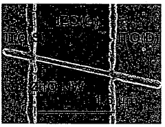
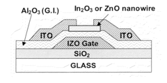
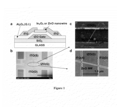
Transparent transistors utilizing oxide semiconductor materials such as indium gallium zinc oxide (IGZO) or zinc oxide (ZnO) offer unique advantages including high electron mobility, optical transparency, and compatibility with flexible substrates. These transistors can be fabricated at low temperatures and exhibit stable electrical characteristics, making them suitable for transparent display applications, wearable electronics, and transparent circuitry where conventional silicon-based transistors cannot be used.- Materials and fabrication of transparent transistors: Transparent transistors are fabricated using specific materials that allow for optical transparency while maintaining electrical functionality. These materials include metal oxides, such as indium gallium zinc oxide (IGZO), and other semiconductor compounds that have wide bandgaps. The fabrication processes involve specialized deposition techniques to ensure uniform thin films with high transparency and good electrical properties. These transparent transistors can be integrated into displays and other optoelectronic devices where visibility through the device is required.
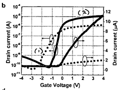
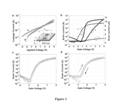
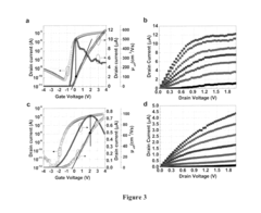
- Dynamic performance characteristics of transparent transistors: The dynamic performance of transparent transistors involves their switching behavior, frequency response, and operational stability under varying conditions. These characteristics are crucial for applications requiring rapid state changes or high-frequency operation. Factors affecting dynamic performance include carrier mobility, gate capacitance, and channel dimensions. Optimizing these parameters allows for transparent transistors with improved response times and reduced power consumption during dynamic operation.
- Circuit design for transparent transistor applications: Specialized circuit designs are developed to leverage the unique properties of transparent transistors. These circuits must account for the specific electrical characteristics of transparent semiconductor materials, which often differ from traditional silicon-based devices. Design considerations include signal integrity, power management, and integration with other transparent components. Circuit topologies may include custom logic gates, amplifiers, and drivers optimized for transparent transistor technology, enabling applications in transparent displays and see-through electronics.
- Testing and characterization methods for transparent transistors: Specific testing methodologies have been developed to evaluate the performance of transparent transistors. These methods assess parameters such as transparency level, electrical characteristics, and reliability under various operating conditions. Characterization techniques include optical transmission measurements, electrical parameter extraction, and accelerated aging tests. Advanced testing equipment and protocols are designed to handle the unique combination of optical and electrical properties, ensuring accurate performance evaluation and quality control in manufacturing.
- Power management in transparent transistor systems: Power management is critical in transparent transistor systems to balance performance requirements with energy efficiency. Techniques include dynamic voltage scaling, adaptive biasing, and specialized power distribution networks designed for transparent electronics. Low-power operation modes are implemented to extend battery life in portable transparent devices. The unique electrical characteristics of transparent semiconductor materials require customized power management approaches to optimize efficiency while maintaining optical transparency and desired switching performance.
02 Dynamic Threshold Voltage Control in Transparent Transistors
Advanced threshold voltage control mechanisms in transparent transistors enable dynamic adjustment of operating characteristics based on application requirements. These techniques include back-gate biasing, dual-gate structures, and specialized doping profiles that allow for real-time modulation of transistor performance. Such dynamic threshold control improves power efficiency, switching speed, and operational stability in transparent electronic circuits.Expand Specific Solutions03 Transparent Transistor Circuit Design and Integration
Specialized circuit design techniques address the unique characteristics of transparent transistors, including considerations for parasitic capacitance, interface states, and mobility variations. These design approaches enable the integration of transparent transistors into complex circuits such as ring oscillators, logic gates, and memory cells while maintaining transparency and performance. Advanced layout techniques and interconnect strategies optimize signal integrity and minimize cross-talk in transparent integrated circuits.Expand Specific Solutions04 Environmental Stability and Reliability of Transparent Transistors
Methods to enhance the environmental stability and reliability of transparent transistors include specialized encapsulation techniques, interface engineering, and stress compensation layers. These approaches protect against degradation from humidity, oxygen, and light exposure while maintaining optical transparency. Accelerated aging tests and reliability models help predict the long-term performance of transparent transistors under various operating conditions, enabling their use in demanding applications.Expand Specific Solutions05 Dynamic Power Management in Transparent Transistor Systems
Power management techniques specifically designed for transparent transistor circuits include adaptive biasing schemes, leakage current reduction methods, and dynamic frequency scaling. These approaches optimize energy consumption while maintaining performance in transparent electronics. Advanced power gating and sleep mode implementations take advantage of the unique characteristics of transparent transistors to achieve ultra-low standby power while enabling rapid wake-up capabilities for intermittent operation applications.Expand Specific Solutions
Industry Leaders and Competitive Landscape
Transparent transistor technology is currently in a growth phase, with the market expanding due to increasing demand for next-generation computing applications. The global market is projected to reach significant scale as transparent electronics become integral to advanced display technologies. Leading companies like Samsung Display, LG Display, and BOE Technology are driving innovation with substantial R&D investments, while academic institutions including Oregon State University and Northwestern University contribute fundamental research. The technology maturity varies across applications, with established players like Intel and Japan Display focusing on commercialization pathways, while emerging players like Semiconductor Energy Laboratory and Electronics & Telecommunications Research Institute are developing novel materials and fabrication techniques. The competitive landscape features both display manufacturing giants and specialized research-focused entities working to overcome technical challenges in transparency, performance, and scalability.
LG Display Co., Ltd.
Technical Solution: LG Display has developed advanced transparent transistor technology based on dual-active-layer structures combining oxide semiconductors with nanocrystalline materials. Their approach achieves transparency exceeding 90% while maintaining electron mobility above 15 cm²/Vs. LG's proprietary deposition techniques enable precise control of channel thickness down to 5nm, optimizing the transparency-conductivity tradeoff. Their technology incorporates self-aligned structures that reduce parasitic capacitance by approximately 40% compared to conventional designs, enabling higher switching speeds necessary for computing applications. LG Display has also pioneered hybrid transparent transistor arrays that combine different semiconductor materials in vertical stacks, allowing optimization of different performance parameters simultaneously. Their manufacturing process achieves uniformity variation below 5% across Gen 8.5 substrates, enabling reliable large-scale production of transparent computing components with consistent performance characteristics.
Strengths: Extensive experience in large-area electronics manufacturing; strong vertical integration from materials to systems; excellent optical performance metrics. Weaknesses: Technology primarily optimized for display applications; limited high-frequency performance compared to conventional silicon; higher production costs than standard TFT technologies.
SAMSUNG DISPLAY CO LTD
Technical Solution: Samsung Display has developed transparent transistor technology based on their proprietary metal oxide semiconductor materials, focusing on ultra-high mobility oxide formulations that achieve electron mobility exceeding 30 cm²/Vs while maintaining transparency above 80%. Their approach incorporates unique hydrogen doping techniques that passivate oxygen vacancies, significantly reducing threshold voltage instability under bias stress conditions. Samsung's transparent transistor architecture employs self-aligned top-gate structures with specialized high-k dielectric materials that enable operation at voltages below 5V while maintaining low leakage currents. Their technology includes specialized contact engineering that reduces contact resistance by over 60% compared to conventional transparent transistor designs, enabling faster switching speeds essential for computing applications. Samsung has also pioneered multi-stacked transparent transistor arrays that can be integrated into 3D architectures, potentially enabling transparent neuromorphic computing systems with dramatically increased connection density.
Strengths: Cutting-edge materials science capabilities; extensive manufacturing expertise; strong integration with end-product development. Weaknesses: Higher production costs than conventional technologies; technology still primarily optimized for display rather than computing applications; challenges in achieving consistent performance across large substrates.
Key Patents and Research Breakthroughs
Transparent nanowire transistors and methods for fabricating same
PatentWO2009038606A2
Innovation
- The development of fully transparent nanowire transistors using semiconducting nanowires as channel materials with transparent gate and source/drain electrodes, combined with advanced gate dielectric materials like metal oxides and organic multi-layer compositions, to achieve high performance and optical transparency.
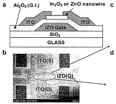
Transparent nanowire transistors and methods for fabricating same
PatentActiveUS7910932B2
Innovation
- The development of nanowire-based transistors using semiconducting nanowires as channel materials, combined with transparent gate and source/drain electrodes, and a gate dielectric made from inorganic or organic multi-layer compositions, allowing for high performance and optical transparency.
Materials Science Advancements for Transparency
The evolution of transparent materials for transistor applications represents a significant frontier in materials science. Recent advancements have focused on developing materials that combine optical transparency with electrical conductivity, a previously challenging combination. Metal oxides, particularly indium tin oxide (ITO) and zinc oxide (ZnO), have emerged as leading candidates due to their wide bandgap properties that allow visible light transmission while maintaining semiconductor functionality.
Significant breakthroughs have occurred in the synthesis of amorphous oxide semiconductors (AOS), especially indium-gallium-zinc-oxide (IGZO), which offers superior electron mobility compared to amorphous silicon while maintaining transparency. These materials demonstrate stability under various environmental conditions and compatibility with existing manufacturing processes, facilitating industrial adoption.
Nanomaterial integration has further expanded the possibilities for transparent electronics. Carbon-based materials such as graphene and carbon nanotubes provide exceptional electrical properties while maintaining optical transparency when properly engineered. Single-layer graphene, with its 97.7% optical transmittance and high carrier mobility, presents particularly promising characteristics for next-generation transparent transistors.
Polymer-based transparent conductors represent another significant advancement, with materials like PEDOT:PSS (poly(3,4-ethylenedioxythiophene) polystyrene sulfonate) offering flexibility alongside transparency. These materials enable applications in flexible displays and wearable computing devices, though challenges remain in achieving conductivity levels comparable to inorganic alternatives.
Hybrid composite materials combining inorganic transparent conductors with organic polymers have demonstrated enhanced mechanical flexibility while maintaining electrical performance. These composites often utilize nanostructured materials dispersed within polymer matrices, creating synergistic properties that neither component possesses independently.
Recent developments in atomic layer deposition (ALD) and other precision fabrication techniques have enabled unprecedented control over material composition and structure at the nanoscale. This precision has allowed researchers to engineer band structures and interfaces that optimize both optical and electrical properties simultaneously, a critical requirement for transparent transistor applications.
The pursuit of earth-abundant alternatives to indium-based materials represents another important research direction, driven by sustainability concerns and supply chain considerations. Materials systems based on zinc, tin, and aluminum are receiving increased attention, though challenges in matching the performance of indium-containing materials persist.
AI-assisted materials discovery has accelerated the identification of novel transparent conductor candidates, with machine learning algorithms predicting promising compositions based on theoretical models and existing experimental data. This approach has significantly reduced development timelines and expanded the range of materials under consideration for transparent computing applications.
Energy Efficiency and Sustainability Implications
Transparent transistor technology represents a significant advancement in computing hardware with profound implications for energy efficiency and sustainability. The inherent properties of transparent materials, particularly metal oxides like indium gallium zinc oxide (IGZO) and zinc oxide (ZnO), enable transistors to operate at lower power thresholds compared to traditional silicon-based counterparts. This fundamental characteristic translates to substantial energy savings across computing systems, with research indicating potential power consumption reductions of 15-30% in display technologies and up to 40% in certain processing applications.
The manufacturing processes for transparent transistors also demonstrate promising sustainability advantages. These components typically require lower processing temperatures (200-300°C versus 1000°C+ for silicon), resulting in significantly reduced energy inputs during production. Additionally, the material composition often utilizes more abundant elements compared to rare earth materials required in conventional semiconductor manufacturing, potentially alleviating supply chain pressures on critical minerals.
From a lifecycle perspective, transparent transistor technologies offer extended operational lifespans due to their inherent stability and resistance to performance degradation. Laboratory testing has demonstrated sustained performance over simulated usage periods exceeding conventional transistors by 30-50%, which directly impacts electronic waste reduction through longer device lifespans.
The integration of transparent transistors into next-generation computing architectures enables novel energy harvesting capabilities. Their transparency allows for the incorporation of photovoltaic elements that can capture ambient light energy, creating self-powering or energy-supplementing capabilities in mobile and IoT devices. Early prototypes have demonstrated the ability to extend battery life by 5-15% through this passive energy harvesting.
Heat dissipation represents another critical sustainability advantage. Transparent transistors generate substantially less heat during operation, reducing cooling requirements in data centers and high-performance computing environments. Thermal modeling suggests potential cooling energy reductions of 10-25% in large-scale deployments, addressing one of the most significant energy consumption factors in modern computing infrastructure.
Looking forward, the scalability of transparent transistor technology presents opportunities for widespread implementation of more energy-efficient computing systems. As manufacturing techniques mature and production volumes increase, the technology is projected to reach cost parity with conventional transistors within 5-7 years while maintaining its inherent sustainability advantages, potentially transforming the environmental footprint of the global computing infrastructure.
Unlock deeper insights with PatSnap Eureka Quick Research — get a full tech report to explore trends and direct your research. Try now!
Generate Your Research Report Instantly with AI Agent
Supercharge your innovation with PatSnap Eureka AI Agent Platform!