Transparent Transistor Market Insights: Challenges and Solutions
OCT 21, 20259 MIN READ
Generate Your Research Report Instantly with AI Agent
Patsnap Eureka helps you evaluate technical feasibility & market potential.
Transparent Transistor Evolution and Objectives
Transparent transistors have evolved significantly since their inception in the early 2000s, marking a revolutionary advancement in display and electronics technology. Initially developed as an alternative to conventional silicon-based transistors, these devices utilize transparent conducting oxide (TCO) materials such as indium gallium zinc oxide (IGZO), zinc oxide (ZnO), and indium tin oxide (ITO). The fundamental breakthrough came with the realization that these materials could maintain electrical conductivity while allowing visible light to pass through, opening unprecedented possibilities for transparent electronics.
The evolution trajectory of transparent transistors has been characterized by several key milestones. The first generation focused primarily on proof-of-concept designs with limited performance metrics. By the mid-2000s, researchers achieved significant improvements in carrier mobility and operational stability, enabling practical applications in display technologies. The 2010s witnessed the commercial integration of transparent transistors in high-resolution displays, particularly through IGZO technology pioneered by companies like Sharp and LG.
Recent developments have expanded beyond traditional metal oxides to include emerging materials such as graphene, carbon nanotubes, and organic semiconductors, each offering unique advantages in flexibility, processing temperature, and environmental stability. This diversification has broadened the application scope from rigid displays to flexible, wearable, and even stretchable electronics.
The primary technical objectives in transparent transistor development currently focus on several critical parameters. First is enhancing carrier mobility while maintaining optical transparency, with researchers targeting mobility values exceeding 100 cm²/Vs without compromising the >80% transparency requirement. Second is improving operational stability under various environmental conditions, particularly humidity and temperature fluctuations that have historically plagued oxide semiconductor performance.
Manufacturing scalability represents another crucial objective, with emphasis on developing low-temperature processes compatible with flexible substrates and roll-to-roll manufacturing. This includes exploration of solution-processing methods that could dramatically reduce production costs compared to vacuum-based deposition techniques currently dominating the industry.
Energy efficiency has emerged as a paramount concern, with research directed toward reducing operating voltages below 1V and minimizing leakage currents. These improvements are essential for battery-powered applications and align with global sustainability initiatives in electronics manufacturing.
The long-term vision for transparent transistor technology extends beyond displays to encompass transparent integrated circuits, smart windows with embedded electronics, augmented reality interfaces, and transparent sensors integrated into everyday objects, supporting the evolution toward ubiquitous computing environments and Internet of Things ecosystems.
Market Demand Analysis for Transparent Electronics
The transparent electronics market has witnessed significant growth in recent years, driven by increasing demand for innovative display technologies and smart devices. Market research indicates that the global transparent electronics market is projected to reach $8.5 billion by 2026, growing at a compound annual growth rate of 21.3% from 2021. This remarkable growth trajectory is primarily fueled by the expanding applications of transparent transistors in consumer electronics, automotive displays, and emerging smart technologies.
Consumer electronics represents the largest segment for transparent electronics, accounting for approximately 45% of the total market share. The demand for transparent displays in smartphones, tablets, and wearable devices continues to rise as manufacturers seek to differentiate their products through innovative form factors and enhanced user experiences. Major smartphone manufacturers have already begun incorporating semi-transparent display elements in their premium devices, signaling a shift toward more immersive and interactive interfaces.
The automotive sector presents another significant growth opportunity for transparent electronics. Heads-up displays (HUDs) utilizing transparent transistor technology are becoming increasingly common in mid-range and premium vehicles. Market analysis shows that automotive applications of transparent electronics are growing at 24.7% annually, outpacing the overall market growth rate. This acceleration is driven by consumer preference for enhanced safety features and the automotive industry's push toward more sophisticated driver assistance systems.
Smart buildings and architectural applications represent an emerging but rapidly expanding market segment. Transparent solar cells, smart windows, and interactive architectural elements are gaining traction in commercial construction projects. The building-integrated photovoltaics segment utilizing transparent electronics is expected to grow by 30% annually over the next five years, reflecting the increasing focus on sustainable and energy-efficient building solutions.
Regional analysis reveals that Asia-Pacific dominates the transparent electronics market, accounting for 38% of global demand, followed by North America (27%) and Europe (24%). China and South Korea lead manufacturing capacity, while Japan maintains technological leadership in several key component categories. The concentration of display manufacturing facilities in East Asia continues to influence the geographic distribution of the transparent electronics supply chain.
Retail and advertising applications represent another promising growth area, with transparent digital signage solutions gaining popularity in high-end retail environments. Market surveys indicate that 72% of retail decision-makers consider transparent display technologies as important differentiators for creating immersive shopping experiences. This trend is particularly pronounced in luxury retail segments, where brand experience and visual merchandising play crucial roles in consumer engagement.
Technical Barriers and Global Development Status
Transparent transistors represent a significant technological advancement in the field of electronics, yet their widespread adoption faces several technical barriers. The primary challenge lies in achieving high electron mobility while maintaining optical transparency. Current transparent conductive oxides (TCOs) like indium tin oxide (ITO) and zinc oxide (ZnO) demonstrate limited carrier mobility compared to silicon-based transistors, restricting their application in high-performance circuits. Additionally, the trade-off between transparency and conductivity remains a fundamental obstacle, as increasing carrier concentration typically reduces optical transparency.
Manufacturing scalability presents another significant barrier. Conventional deposition methods for transparent semiconductors, such as pulsed laser deposition and sputtering, often struggle with uniformity across large areas, limiting industrial-scale production. The stability of these devices under environmental conditions also poses challenges, with many transparent semiconductors exhibiting sensitivity to oxygen, moisture, and light exposure, leading to performance degradation over time.
Globally, research and development in transparent transistor technology shows distinct regional patterns. Japan and South Korea lead in industrial applications, with companies like Samsung and LG investing heavily in transparent display technologies. These nations have established robust patent portfolios and manufacturing capabilities for oxide semiconductor-based transistors, particularly focusing on indium gallium zinc oxide (IGZO) technology.
The United States maintains strength in fundamental research, with institutions like MIT and Stanford University pioneering novel materials and device architectures. European research centers, particularly in Germany and the UK, focus on sustainable alternatives to indium-based materials, addressing concerns about indium scarcity and environmental impact.
China has rapidly emerged as a significant player, combining government-backed research initiatives with manufacturing capabilities. Chinese institutions have made notable advances in low-temperature processing techniques and flexible transparent electronics, positioning the country as a growing force in this field.
Recent technological breakthroughs include the development of solution-processed transparent transistors, which offer cost-effective manufacturing routes, and the integration of 2D materials like graphene and MoS2, which promise enhanced electrical properties while maintaining transparency. However, these approaches remain largely confined to laboratory settings, with significant work needed to achieve commercial viability.
The standardization of testing protocols and performance metrics represents another challenge in the field. Different research groups and manufacturers employ varying methods to measure transparency, mobility, and stability, making direct comparisons difficult and potentially slowing industry-wide progress. International collaboration on standardization efforts has begun but remains in early stages.
Current Solutions in Transparent Transistor Fabrication
01 Transparent oxide semiconductor materials for transistors
Various oxide semiconductor materials can be used to create transparent transistors. These materials, such as zinc oxide (ZnO), indium gallium zinc oxide (IGZO), and other metal oxides, offer high electron mobility while maintaining optical transparency. The combination of these properties makes them ideal for applications requiring both electrical functionality and visual transparency, such as displays and smart windows.- Transparent oxide semiconductor materials for transistors: Transparent transistors can be fabricated using oxide semiconductor materials such as indium gallium zinc oxide (IGZO), zinc oxide (ZnO), or tin oxide (SnO2). These materials offer high electron mobility while maintaining optical transparency in the visible spectrum. The use of these oxide semiconductors enables the creation of transistors that can be integrated into transparent electronic devices, displays, and sensors without compromising visibility or optical performance.
- Transparent electrode materials and structures: Transparent electrodes are essential components of transparent transistors, typically made from materials like indium tin oxide (ITO), aluminum-doped zinc oxide (AZO), or graphene. These electrodes need to balance electrical conductivity with optical transparency. Advanced structures such as mesh electrodes, nanowire networks, or ultrathin metal films can be employed to optimize this balance. The design and composition of these electrodes significantly impact the overall transparency and performance of the transistor.
- Transparent substrate and dielectric materials: The choice of substrate and dielectric materials is crucial for transparent transistor fabrication. Common transparent substrates include glass, flexible polymers like polyethylene terephthalate (PET), and more recently developed materials such as transparent polyimides. Dielectric layers made from materials like silicon dioxide, aluminum oxide, or organic insulators must maintain transparency while providing good electrical insulation properties. These materials enable the creation of fully transparent transistor structures for applications in transparent electronics.
- Fabrication techniques for transparent transistors: Various fabrication techniques are employed to create transparent transistors while maintaining optical clarity. These include low-temperature deposition methods such as sputtering, solution processing, and atomic layer deposition that preserve substrate transparency. Patterning techniques like photolithography with transparent photoresists or direct laser writing help create precise transistor structures. Advanced manufacturing approaches such as roll-to-roll processing enable mass production of transparent transistors on flexible substrates for next-generation transparent electronics.
- Applications and integration of transparent transistors: Transparent transistors find applications in various fields including transparent displays, smart windows, augmented reality devices, and transparent sensors. Integration techniques focus on connecting transparent transistors with other transparent components to create fully transparent electronic systems. Circuit design considerations for transparent transistors address unique challenges related to optical transparency requirements while maintaining electrical performance. These applications demonstrate the practical utility of transparent transistor technology in creating visually unobtrusive electronic devices.
02 Transparent electrode materials and structures
Transparent electrodes are crucial components in transparent transistor technology. Materials such as indium tin oxide (ITO), graphene, and silver nanowires can be used to create electrodes that conduct electricity while allowing light to pass through. The structure and deposition methods of these electrodes significantly impact the overall transparency and performance of the transistor devices.Expand Specific Solutions03 Transparent substrate technologies
Transparent substrates serve as the foundation for transparent transistors. Materials like glass, flexible polymers, and certain crystalline materials can be used as substrates that maintain transparency while providing mechanical support. The choice of substrate affects not only the optical properties but also the fabrication process, durability, and potential applications of the transparent transistors.Expand Specific Solutions04 Transparency enhancement techniques
Various techniques can be employed to enhance the transparency of transistors. These include optimizing layer thicknesses, using anti-reflection coatings, implementing nano-structured surfaces, and developing novel device architectures. These approaches minimize light absorption and scattering, resulting in improved overall transparency while maintaining electrical performance.Expand Specific Solutions05 Applications of transparent transistor technology
Transparent transistors enable numerous innovative applications across various industries. They are essential components in transparent displays, smart windows, augmented reality devices, and transparent electronics. The ability to create circuits that are invisible to the human eye opens possibilities for integrating electronics into everyday objects without altering their appearance, leading to advancements in consumer electronics, automotive, and architectural applications.Expand Specific Solutions
Industry Leaders and Competitive Landscape
The transparent transistor market is currently in a growth phase, characterized by increasing demand for transparent display technologies across various sectors. The market size is expanding steadily, driven by applications in consumer electronics, automotive displays, and smart devices. From a technological maturity perspective, the field shows varying levels of development among key players. Research institutions like Oregon State University, Tokyo Institute of Technology, and MIT are pioneering fundamental innovations, while commercial entities including BOE Technology, Samsung Electronics, and Sharp Corp. are focusing on practical applications and mass production capabilities. Companies like E Ink Holdings (formerly Prime View International) and Semiconductor Energy Laboratory are advancing specialized applications in e-paper and OLED technologies, respectively. The competitive landscape reveals a balance between academic research and industrial implementation, with Asian manufacturers currently holding significant market share.
Oregon State University
Technical Solution: Oregon State University has pioneered fundamental research in transparent transistor technology, particularly focusing on amorphous oxide semiconductors. Their approach centers on zinc tin oxide (ZTO) materials that avoid the use of indium, addressing cost and supply concerns associated with ITO and IGZO. OSU's research has developed novel solution-processing methods for transparent transistors, including spin-coating and inkjet printing of precursor solutions followed by optimized annealing protocols. These methods achieve mobility values of 5-8 cm²/Vs while maintaining transparency above 80%. Their transistor architecture incorporates innovative dielectric materials, including aluminum oxide and zirconium oxide layers deposited via atomic layer deposition (ALD), resulting in improved interface quality and reduced trap states. OSU has demonstrated transparent transistors on flexible substrates including PET and paper, with operational stability maintained after 1000+ bending cycles. Their research has also explored complementary device structures using both n-type and p-type transparent semiconductors, a critical advancement toward transparent integrated circuits.
Strengths: Pioneering fundamental research that has established many core principles of transparent electronics, innovative approaches to materials and processing that reduce costs, and strong focus on environmentally friendly materials and processes. Weaknesses: Technologies generally at lower technology readiness levels compared to commercial entities, challenges in scaling laboratory processes to production volumes, and performance metrics that sometimes lag behind leading commercial implementations.
BOE Technology Group Co., Ltd.
Technical Solution: BOE has developed a comprehensive transparent transistor technology platform based on amorphous oxide semiconductors, primarily IGZO and ITZO (Indium Tin Zinc Oxide). Their approach focuses on large-area uniformity, achieving less than 5% variation in electrical characteristics across Gen 10.5 substrates (2940×3370mm). BOE's transparent transistors feature a bottom-gate, top-contact architecture with specially engineered source/drain electrodes using ITO/Ag/ITO multilayer structures that balance conductivity and transparency. Their manufacturing process employs low-temperature (200°C) PECVD for dielectric layers and optimized annealing sequences that enhance carrier mobility while maintaining transparency above 80%. BOE has successfully implemented these transistors in commercial transparent display products, achieving pixel densities of 400+ PPI with aperture ratios exceeding 60%. Their technology incorporates compensation circuits that minimize image sticking and threshold voltage shifts, resulting in operational stability exceeding 10,000 hours under continuous use conditions.
Strengths: Exceptional large-area manufacturing capability, established supply chain for materials, strong integration with display production, and cost-effective scaling. BOE's vertical integration allows for rapid implementation in commercial products. Weaknesses: Somewhat lower mobility compared to leading research prototypes, challenges with long-term stability in high-humidity environments, and higher defect densities compared to smaller-scale production.
Key Patents and Technical Innovations
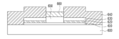
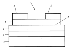
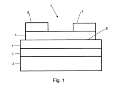
Method of manufacturing transparent transistor with multi-layered structures
PatentInactiveUS20120315729A1
Innovation
- A stacked structure for transparent transistors is implemented, comprising a substrate with source and drain electrodes having a multi-layered structure of a lower transparent layer, a metal layer, and an upper transparent layer, where the lower and upper transparent layers are formed of the same transparent semiconductor material, and a gate electrode is aligned with the channel, potentially including nitride layers for enhanced refractive index and conductivity.
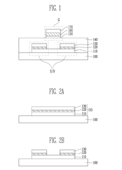
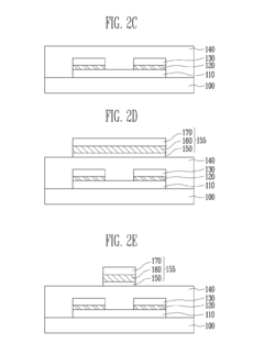
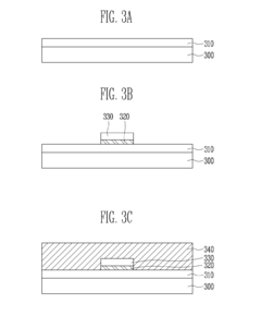
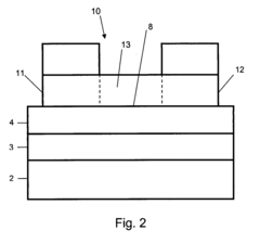
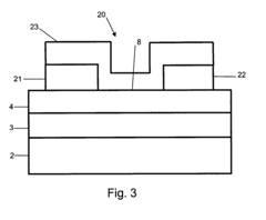
Transistor structures and methods for making the same
PatentInactiveUS20070141784A1
Innovation
- Development of enhancement-mode, field-effect transistors with a substantially transparent channel layer made from materials like ZnO or SnO2, which are produced by annealing, and a gate insulator layer, allowing for a transparent transistor structure that enables high optical transmission across the visible and infrared spectrum.
Supply Chain Analysis and Manufacturing Challenges
The transparent transistor supply chain presents a complex ecosystem with multiple critical dependencies and manufacturing challenges. Raw material sourcing remains a fundamental concern, with indium tin oxide (ITO) and zinc oxide serving as primary materials for transparent conductive layers. The limited availability of indium, particularly, has created supply vulnerabilities, with over 70% of global production concentrated in China. This geographic concentration introduces significant geopolitical risks and price volatility that manufacturers must navigate.
Manufacturing processes for transparent transistors demand specialized equipment and ultra-clean environments, creating substantial barriers to entry. The production of high-quality transparent oxide semiconductors requires precise control of deposition parameters, with even minor variations potentially resulting in performance inconsistencies. This precision requirement has led to manufacturing yield challenges, with industry reports suggesting average yields between 60-75% for high-performance transparent transistor arrays.
Equipment suppliers represent another critical link in the supply chain, with companies like Applied Materials, Tokyo Electron, and ULVAC dominating the market for specialized deposition systems. The concentration of equipment expertise creates potential bottlenecks, especially during periods of rapid demand growth. Additionally, the specialized nature of this equipment contributes to high capital expenditure requirements for new market entrants.
Scaling production presents significant technical hurdles, particularly in achieving uniform electrical characteristics across large substrate areas. While small-scale laboratory demonstrations have achieved impressive performance metrics, translating these results to mass production remains challenging. The industry continues to struggle with balancing performance, yield, and cost at commercial scales.
Integration challenges further complicate the supply chain, as transparent transistors must interface seamlessly with other components in display systems or sensor arrays. This integration often requires specialized packaging solutions and interconnect technologies that can maintain transparency while providing reliable electrical connections. The development of these supporting technologies has not always kept pace with advances in transistor performance.
Environmental considerations are increasingly impacting supply chain decisions, with regulations on hazardous materials and energy consumption becoming more stringent. Manufacturers are exploring alternative materials and more efficient production processes to address these concerns, though many alternatives currently offer reduced performance or higher costs compared to established solutions.
Sustainability and Environmental Impact Assessment
The environmental footprint of transparent transistor technologies has become increasingly significant as these components find wider applications in consumer electronics, smart displays, and renewable energy systems. Current manufacturing processes for transparent transistors often involve rare earth elements and energy-intensive fabrication methods that raise sustainability concerns. The extraction of indium, a critical material in indium tin oxide (ITO) - the most commonly used transparent conductor - has been linked to significant environmental degradation and resource depletion, with global reserves estimated to last only 20-30 more years at current consumption rates.
Energy consumption during manufacturing represents another substantial environmental challenge. Conventional transparent transistor production typically requires high-temperature processes and vacuum deposition techniques that consume considerable energy. Recent life cycle assessments indicate that the carbon footprint of a single square meter of transparent electronic components can be equivalent to that of producing several kilograms of plastic, highlighting the need for more efficient production methods.
Chemical waste management presents additional environmental concerns. The etching processes used in transistor fabrication generate hazardous waste containing heavy metals and toxic compounds that require specialized disposal procedures. Industry reports suggest that for every square meter of transparent electronics produced, approximately 30-40 liters of contaminated wastewater may be generated, creating significant treatment challenges.
Encouragingly, several sustainable alternatives are emerging within the industry. Solution-processed metal oxide semiconductors have demonstrated potential to reduce energy consumption by up to 40% compared to vacuum-based methods. These approaches operate at lower temperatures and eliminate the need for energy-intensive vacuum equipment, substantially reducing the carbon footprint of production facilities.
Biodegradable and recyclable substrate materials represent another promising development. Research teams have successfully demonstrated transparent transistors on cellulose-based substrates that can be composted at end-of-life, potentially addressing the growing electronic waste crisis. These bio-based alternatives could reduce the environmental impact of disposable electronic devices and sensors.
Circular economy initiatives are also gaining traction among leading manufacturers. Companies are implementing take-back programs for transparent display components and developing modular designs that facilitate repair and material recovery. These approaches could extend product lifespans and improve resource efficiency throughout the value chain, though widespread adoption remains limited by economic and logistical barriers.
Unlock deeper insights with Patsnap Eureka Quick Research — get a full tech report to explore trends and direct your research. Try now!
Generate Your Research Report Instantly with AI Agent
Supercharge your innovation with Patsnap Eureka AI Agent Platform!