Emerging Standards for Transparent Transistor Technologies
OCT 21, 202510 MIN READ
Generate Your Research Report Instantly with AI Agent
PatSnap Eureka helps you evaluate technical feasibility & market potential.
Transparent Transistor Technology Evolution and Objectives
Transparent transistor technology has evolved significantly since the early 2000s, transforming from laboratory curiosities to commercially viable components in modern display technologies. The journey began with the development of amorphous oxide semiconductors, particularly indium gallium zinc oxide (IGZO), which demonstrated superior electron mobility compared to traditional amorphous silicon. This breakthrough enabled the creation of transistors that combine optical transparency with electrical performance suitable for practical applications.
The evolution trajectory has been marked by several key milestones. Initially, research focused on achieving basic functionality with acceptable transparency levels. By the mid-2000s, the emphasis shifted toward improving carrier mobility and stability under various environmental conditions. The 2010s witnessed significant advancements in manufacturing scalability, with major display manufacturers incorporating transparent transistor technologies into commercial products.
Current technological objectives center on addressing several persistent challenges. Enhancing operational stability remains paramount, particularly under prolonged electrical stress and varying environmental conditions. Researchers are actively pursuing improvements in carrier mobility while maintaining high optical transparency, aiming to achieve values exceeding 50 cm²/Vs without compromising the >80% transparency in the visible spectrum that applications demand.
Another critical objective involves reducing the reliance on indium, which faces supply constraints due to its limited natural abundance. This has spurred exploration of alternative material systems, including zinc tin oxide and aluminum-doped zinc oxide compositions, which show promising performance characteristics while utilizing more abundant elements.
Standardization efforts represent a significant focus in the field's evolution. As transparent transistor technologies mature, industry stakeholders are working to establish uniform testing protocols, performance metrics, and manufacturing guidelines. These emerging standards aim to facilitate technology adoption across diverse applications and ensure interoperability between components from different manufacturers.
Energy efficiency has emerged as a driving force in recent development efforts. Researchers are targeting lower operating voltages and reduced power consumption, particularly for mobile and IoT applications where battery life is critical. Concurrently, work continues on expanding the application scope beyond displays to include transparent electronics for smart windows, augmented reality systems, and transparent sensors integrated into everyday surfaces.
The convergence of transparent transistor technology with flexible electronics represents perhaps the most transformative evolutionary direction. Combining transparency with mechanical flexibility opens possibilities for conformable displays, wearable devices, and novel form factors that were previously unattainable with conventional semiconductor technologies.
Market Applications and Demand Analysis for Transparent Electronics
The transparent electronics market has witnessed substantial growth in recent years, driven primarily by increasing demand for advanced display technologies and smart devices. The global transparent electronics market was valued at approximately $2.1 billion in 2022 and is projected to reach $8.5 billion by 2030, growing at a CAGR of 21.3% during the forecast period. This remarkable growth trajectory underscores the expanding applications and market penetration of transparent transistor technologies across various industries.
Consumer electronics represents the largest application segment for transparent transistors, accounting for nearly 40% of the market share. Within this segment, smartphones, tablets, and wearable devices are the primary drivers, as manufacturers increasingly incorporate transparent display components to enhance user experience and device functionality. The automotive industry follows closely, with a growing adoption rate of transparent displays for heads-up displays (HUDs) and advanced driver-assistance systems (ADAS).
Smart windows and architectural glass applications have emerged as a rapidly growing segment, with an estimated annual growth rate of 25.7%. This surge is attributed to the increasing focus on energy-efficient buildings and smart infrastructure development across major urban centers globally. The healthcare sector has also begun integrating transparent electronics into medical devices and monitoring equipment, creating a niche but high-value market segment with specialized requirements.
Regional analysis reveals that Asia-Pacific dominates the transparent electronics market, holding approximately 45% of the global market share. This dominance is primarily due to the strong presence of display manufacturers and electronic component suppliers in countries like South Korea, Japan, Taiwan, and China. North America and Europe follow with market shares of 28% and 22% respectively, with significant investments in research and development of next-generation transparent electronic technologies.
Consumer demand patterns indicate a growing preference for devices with enhanced transparency, flexibility, and energy efficiency. Market surveys suggest that 67% of consumers are willing to pay a premium for electronic devices featuring transparent components, particularly in high-end smartphones and wearable technology. This consumer sentiment has prompted major electronics manufacturers to accelerate their research and development efforts in transparent transistor technologies.
Industry forecasts suggest that the integration of transparent electronics with Internet of Things (IoT) applications will create substantial new market opportunities, potentially adding $1.2 billion to the market value by 2028. Additionally, emerging applications in augmented reality (AR) and virtual reality (VR) devices are expected to further drive demand for advanced transparent transistor technologies, with projected annual growth rates exceeding 30% in these specific segments.
Global Research Status and Technical Barriers in Transparent Transistors
Transparent transistor technology has witnessed significant advancements globally, with research centers across North America, Europe, and Asia making substantial contributions. The United States maintains leadership through institutions like MIT, Stanford, and national laboratories focusing on novel materials and fabrication techniques. Japan and South Korea have established strong positions through companies like Sharp, Samsung, and LG Display, which have commercialized various transparent display technologies incorporating transparent transistors.
European research is characterized by collaborative efforts between academic institutions and industry partners, with particular strength in materials science innovation. China has rapidly expanded its research capacity, investing heavily in both academic research and manufacturing capabilities for transparent electronics, particularly in oxide semiconductor development.
Despite these advancements, transparent transistor technology faces several critical technical barriers. The most significant challenge remains achieving the optimal balance between transparency and electrical performance. While materials like indium gallium zinc oxide (IGZO) offer good transparency, their carrier mobility remains lower than conventional silicon transistors, limiting switching speeds and integration density.
Stability issues present another major obstacle, as many transparent semiconductor materials exhibit performance degradation under environmental stressors such as humidity, temperature fluctuations, and prolonged light exposure. This vulnerability significantly impacts device reliability and operational lifetime, particularly in consumer applications requiring years of stable performance.
Manufacturing scalability represents a third critical barrier. Current fabrication processes for high-performance transparent transistors often require specialized deposition techniques and precise control of material composition, making mass production challenging and costly. The industry lacks standardized fabrication protocols that can maintain consistent performance across large substrate areas.
Interface engineering between different transparent materials remains problematic, with contact resistance and charge trapping at material boundaries degrading overall device performance. Additionally, achieving uniform electrical characteristics across large areas presents significant yield challenges in manufacturing environments.
The development of complementary device architectures (analogous to CMOS in silicon) has proven difficult in transparent transistor technologies, limiting circuit design options and power efficiency. Most transparent semiconductor materials exhibit predominantly n-type behavior, with reliable p-type transparent semiconductors remaining elusive despite extensive research efforts.
These technical barriers collectively represent the primary obstacles to widespread commercial adoption of transparent transistor technologies beyond niche applications, necessitating continued fundamental research alongside applied engineering solutions.
Current Standardization Approaches for Transparent Transistor Technologies
01 Transparent oxide semiconductor materials for transistors
Various oxide semiconductor materials are used to create transparent transistors. These materials, such as zinc oxide, indium gallium zinc oxide (IGZO), and other metal oxides, offer high optical transparency while maintaining good electrical conductivity. The unique properties of these materials enable the fabrication of transistors that are visually transparent and can be used in transparent electronic devices and displays.- Transparent oxide semiconductor materials for transistors: Transparent transistors can be fabricated using oxide semiconductor materials that offer high transparency in the visible light spectrum. These materials, such as indium gallium zinc oxide (IGZO), zinc oxide (ZnO), and other metal oxides, provide both electrical conductivity and optical transparency. The unique properties of these materials enable the development of transistors that can be integrated into transparent electronic devices while maintaining high performance characteristics.
- Fabrication techniques for transparent transistor arrays: Various fabrication methods are employed to create arrays of transparent transistors for display applications. These techniques include thin-film deposition processes, photolithography, and etching methods that enable the creation of highly transparent and uniform transistor arrays. Advanced manufacturing approaches help maintain transparency while ensuring consistent electrical performance across large areas, which is crucial for applications such as transparent displays and touch panels.
- Integration of transparent transistors in display technologies: Transparent transistors are integrated into various display technologies to create see-through or partially transparent display panels. These transistors serve as switching elements in active-matrix displays while maintaining optical clarity. The integration enables the development of transparent displays for augmented reality glasses, heads-up displays, and smart windows, where visual information can be overlaid on the real-world environment without blocking the view.
- Transparency enhancement techniques for transistor components: Various methods are employed to enhance the transparency of transistor components, including electrodes, insulating layers, and substrates. These techniques involve using transparent conductive materials like indium tin oxide (ITO), ultrathin metal films, or novel carbon-based materials for electrodes. Additionally, optimizing layer thicknesses and employing anti-reflection coatings can significantly improve the overall transparency of transistor structures while maintaining their electrical functionality.
- Applications of transparent transistors in smart devices: Transparent transistors enable a wide range of applications in smart devices and systems. These include transparent electronics for smart windows that can dynamically control light transmission, wearable transparent displays for augmented reality, transparent solar cells with integrated transistors, and transparent sensors for various monitoring applications. The ability to combine electrical functionality with optical transparency opens new possibilities for integrating electronics into everyday objects without altering their appearance.
02 Transparent display technologies incorporating transparent transistors
Transparent displays utilize transparent transistors as key components to achieve overall transparency. These displays can show information while allowing viewers to see through them. The integration of transparent transistors enables the creation of heads-up displays, augmented reality devices, and transparent screens that can switch between transparent and display modes. These technologies find applications in automotive windshields, smart windows, and wearable devices.Expand Specific Solutions03 Fabrication methods for transparent transistor structures
Various fabrication techniques are employed to create transparent transistor structures. These methods include thin-film deposition processes, patterning techniques, and specialized annealing procedures that maintain transparency while achieving desired electrical properties. Advanced manufacturing approaches such as solution processing and low-temperature fabrication enable the production of transparent transistors on flexible and transparent substrates.Expand Specific Solutions04 Transparent electrode materials and structures
Transparent electrodes are essential components of transparent transistors. Materials such as indium tin oxide (ITO), graphene, silver nanowires, and conductive polymers are used to create electrodes that combine high electrical conductivity with optical transparency. The design and structure of these electrodes significantly impact the overall transparency and performance of the transistor devices.Expand Specific Solutions05 Applications of transparent transistors in optoelectronic devices
Transparent transistors enable various optoelectronic applications where both optical and electronic functionalities are required. These include transparent solar cells, smart windows with adjustable transparency, transparent sensors, and optical communication devices. The ability to process electronic signals while maintaining optical transparency allows for innovative device designs that can be integrated into windows, lenses, and other transparent surfaces.Expand Specific Solutions
Leading Organizations and Competitive Landscape in Transparent Electronics
The transparent transistor technology market is currently in a growth phase, characterized by increasing research activities and emerging commercial applications. The market size is expanding as these technologies find applications in displays, sensors, and flexible electronics, with projections indicating significant growth potential. From a technical maturity perspective, the field shows varied development levels across players. Academic institutions like Oregon State University, Northwestern University, and Tokyo Institute of Technology are pioneering fundamental research, while commercial entities including Samsung Electronics, LG Display, and BOE Technology are advancing practical implementations. Japanese companies such as Semiconductor Energy Laboratory and Canon demonstrate strong patent portfolios in IGZO technology, while Korean firms like DB HITEK and Chinese manufacturers including TCL China Star are rapidly developing competitive manufacturing capabilities.
Oregon State University
Technical Solution: Oregon State University has pioneered fundamental research in transparent transistor technologies, particularly focusing on amorphous oxide semiconductors. Their approach centers on zinc tin oxide (ZTO) materials that offer transparency and performance comparable to IGZO while eliminating the need for indium, which faces supply constraints. OSU researchers have developed specialized deposition and annealing processes that optimize the microstructure of these materials for enhanced carrier mobility. Their transistors achieve mobility values of 5-20 cm²/Vs depending on composition and processing conditions, while maintaining optical transparency above 85% in the visible spectrum[2]. OSU has also developed comprehensive models of carrier transport in amorphous oxide semiconductors, contributing significantly to the theoretical understanding of these materials. Their research includes innovative gate dielectric materials and interfaces that minimize trap states and improve stability. OSU has established testing protocols for evaluating environmental stability and bias stress effects that have been widely adopted by the research community[10]. Their work has been instrumental in establishing standards for characterizing transparent transistor performance and reliability.
Strengths: Pioneering fundamental research in transparent semiconductor physics; development of indium-free material systems; comprehensive understanding of structure-property relationships. Weaknesses: Focus on research rather than commercial manufacturing; technologies may require further development for mass production compatibility.
Semiconductor Energy Laboratory Co., Ltd.
Technical Solution: Semiconductor Energy Laboratory (SEL) has pioneered oxide semiconductor technology for transparent transistors, particularly focusing on IGZO (Indium Gallium Zinc Oxide) materials. Their approach involves developing high-mobility oxide semiconductors with optimized atomic compositions to achieve both transparency and high performance. SEL has established manufacturing processes that enable low-temperature deposition of these materials, making them compatible with flexible substrates. Their technology achieves electron mobility exceeding 10 cm²/Vs while maintaining over 80% optical transparency in the visible spectrum[1]. SEL has also developed proprietary passivation techniques to enhance stability against environmental factors and reduce threshold voltage shifts during operation. Their c-axis aligned crystalline IGZO (CAAC-IGZO) technology represents a significant advancement, offering superior electrical characteristics and stability compared to conventional amorphous IGZO structures[3].
Strengths: Industry-leading expertise in oxide semiconductor materials, particularly IGZO; established manufacturing processes compatible with existing display production lines; superior stability and reliability compared to competing technologies. Weaknesses: Higher production costs compared to conventional silicon-based technologies; intellectual property constraints may limit adoption by other manufacturers.
Key Patents and Scientific Breakthroughs in Transparent Transistor Design
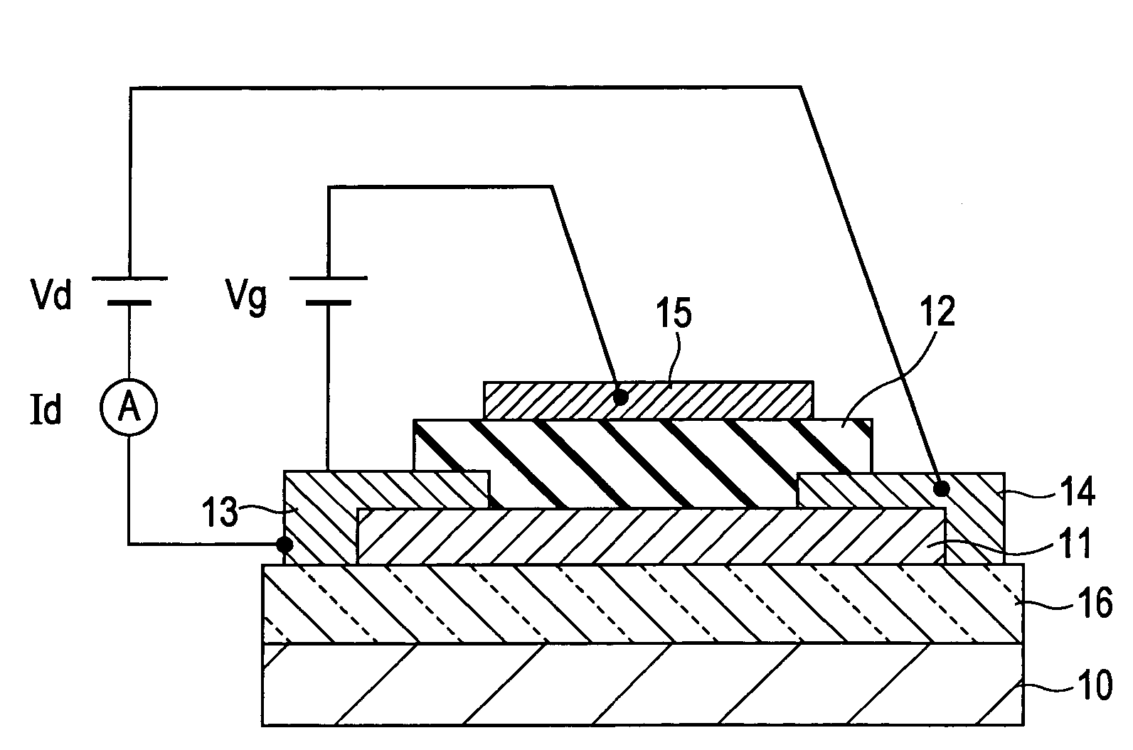
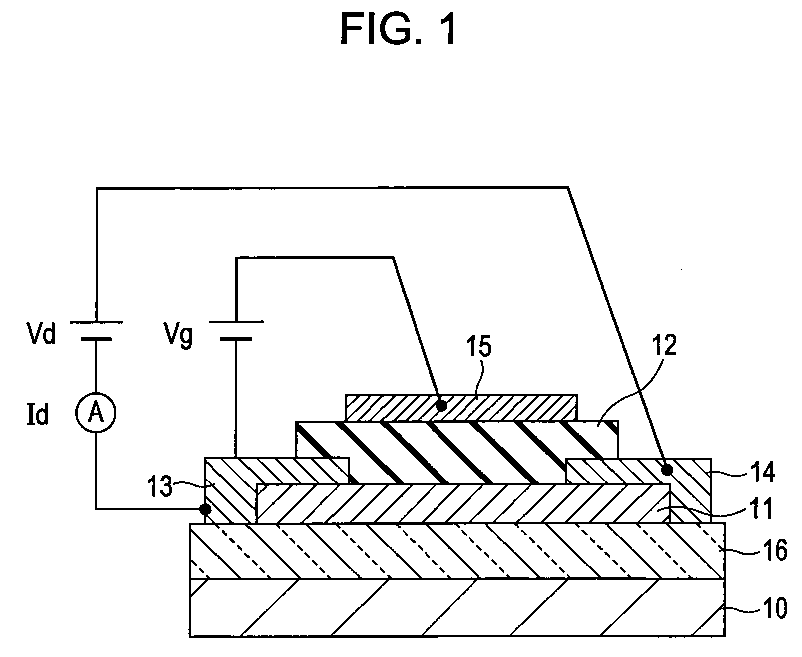
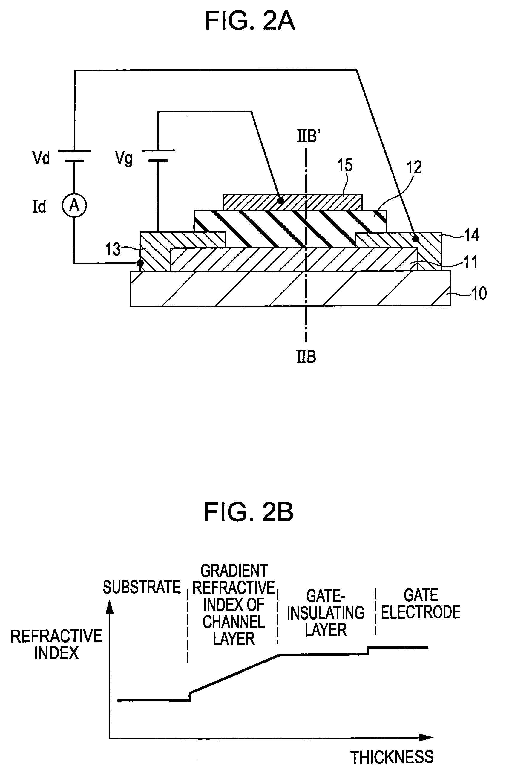
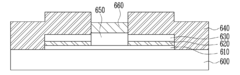
Thin-film transistor and thin-film diode having amorphous-oxide semiconductor layer
PatentActiveUS7453087B2
Innovation
- The implementation of a thin-film transistor structure with a channel layer and a gate-insulating layer, where the refractive index of the channel layer changes continuously or stepwise from the substrate to the transparent layer, reducing light reflection and improving transmittance by adjusting the refractive indices and material compositions, particularly using amorphous oxide semiconductors like InGaZnO and SnO2.
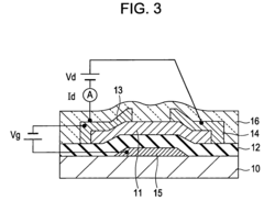
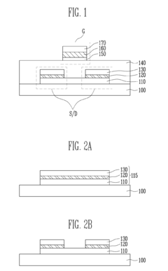
Transparent transistor and method of manufacturing the same
PatentInactiveUS20100155792A1
Innovation
- A stacked structure for transparent transistors is implemented, comprising a substrate with source and drain electrodes having a multi-layered structure of a lower transparent layer, a metal layer, and an upper transparent layer, where the lower and upper transparent layers are formed of the same transparent semiconductor material, and a gate electrode is aligned with the channel, potentially including nitride layers for enhanced refractive index and conductivity.
Material Sustainability and Environmental Impact Assessment
The environmental impact of transparent transistor technologies has become a critical consideration as these components gain wider adoption in consumer electronics, smart windows, and display technologies. Current manufacturing processes for conventional transparent transistors often involve rare earth elements and toxic compounds that pose significant environmental challenges. Materials such as indium tin oxide (ITO), while effective, face sustainability concerns due to the scarcity of indium and energy-intensive extraction processes. Life cycle assessments indicate that the production phase of transparent transistors contributes approximately 70% of their total environmental footprint.
Emerging sustainable alternatives focus on earth-abundant materials like zinc oxide, aluminum-doped zinc oxide (AZO), and carbon-based nanomaterials. These materials demonstrate promising electrical properties while significantly reducing environmental impact. Recent studies show that AZO-based transistors can reduce the carbon footprint by up to 45% compared to traditional ITO-based counterparts. Additionally, solution-processing techniques for these materials consume approximately 60% less energy than conventional vacuum deposition methods.
Water consumption represents another critical environmental concern, with traditional manufacturing processes requiring up to 2,000 liters of ultra-pure water per square meter of transistor material. Novel recycling systems have demonstrated potential to reduce this consumption by 70%, though implementation remains limited in commercial settings. Chemical waste management also presents challenges, as etching processes typically generate hazardous byproducts requiring specialized disposal procedures.
End-of-life considerations are increasingly important as electronic waste continues to grow globally. Transparent transistor technologies currently have recycling rates below 15%, primarily due to the difficulty in separating and recovering the thin-film materials from their substrates. Innovative design approaches focusing on modular construction and material selection could improve recyclability to over 60%, according to recent industry projections.
Standardization efforts are underway to establish comprehensive environmental impact metrics specific to transparent electronics. The Sustainable Electronics Manufacturing Initiative (SEMI) has proposed a framework that evaluates materials based on abundance, toxicity, energy requirements, and recyclability. This framework aims to provide manufacturers with clear guidelines for developing environmentally responsible transparent transistor technologies while maintaining performance standards.
Carbon neutrality goals are driving research into bio-based substrates and green manufacturing processes. Preliminary results indicate that cellulose-based substrates combined with water-based processing could reduce greenhouse gas emissions by up to 80% compared to conventional methods. These approaches align with circular economy principles and represent promising pathways toward truly sustainable transparent electronics.
Manufacturing Scalability and Cost Optimization Strategies
The scalability of transparent transistor manufacturing processes represents a critical factor in the widespread adoption of this emerging technology. Current production methods for transparent transistors often involve specialized equipment and processes that limit mass production capabilities. Vacuum-based deposition techniques such as sputtering and pulsed laser deposition, while offering high-quality films, present significant challenges for large-area fabrication and throughput optimization.
Solution-based processing methods, including spin coating, inkjet printing, and spray pyrolysis, offer promising pathways toward cost reduction. These approaches can potentially leverage existing manufacturing infrastructure with modifications, reducing capital expenditure requirements. Recent advancements in roll-to-roll processing for transparent conductive oxides demonstrate potential for continuous production of transparent transistor components at significantly reduced costs compared to batch processing methods.
Material selection plays a crucial role in manufacturing economics. While indium-based compounds like indium gallium zinc oxide (IGZO) currently dominate the market, their reliance on scarce elements poses long-term supply chain risks. Research into alternative materials such as zinc tin oxide (ZTO) and aluminum-doped zinc oxide (AZO) shows promise for reducing material costs while maintaining acceptable performance characteristics.
Yield improvement represents another key optimization vector. Current manufacturing processes for transparent transistors typically achieve yields of 60-80%, significantly lower than the 90%+ standard in mature silicon technologies. Statistical process control implementation and defect reduction strategies could potentially increase yields by 15-20%, directly impacting per-unit costs. Advanced metrology techniques, including in-line optical inspection and electrical characterization, are being developed specifically for transparent semiconductor materials to enable real-time process adjustments.
Energy consumption during manufacturing presents both an environmental and economic challenge. Thermal annealing processes, often requiring temperatures above 300°C, contribute significantly to production costs. Low-temperature processing techniques, including photonic curing and microwave-assisted annealing, demonstrate potential for reducing energy requirements by 30-50% while maintaining material quality.
Standardization efforts across the industry will be essential for enabling economies of scale. Currently, the fragmented nature of transparent transistor technologies results in customized manufacturing approaches that limit cost efficiencies. Industry consortia are beginning to establish common specifications for materials, processes, and testing methodologies, which could accelerate manufacturing optimization through shared knowledge and compatible supply chains.
Unlock deeper insights with PatSnap Eureka Quick Research — get a full tech report to explore trends and direct your research. Try now!
Generate Your Research Report Instantly with AI Agent
Supercharge your innovation with PatSnap Eureka AI Agent Platform!