Comparative Analysis of Transparent Transistor Efficiency
OCT 21, 202510 MIN READ
Generate Your Research Report Instantly with AI Agent
PatSnap Eureka helps you evaluate technical feasibility & market potential.
Transparent Transistor Evolution and Objectives
Transparent transistors have emerged as a critical technology in modern electronics, evolving significantly since their initial development in the early 2000s. The journey began with amorphous oxide semiconductors, particularly indium gallium zinc oxide (IGZO), which offered improved electron mobility compared to amorphous silicon while maintaining transparency. This breakthrough enabled the first generation of transparent electronic devices with limited but functional performance characteristics.
The evolution accelerated with the introduction of zinc oxide-based transistors, which provided a more environmentally friendly and cost-effective alternative to indium-containing compounds. These developments coincided with the growing demand for transparent displays and touch interfaces in consumer electronics, creating a symbiotic relationship between market pull and technology push factors in the field.
A significant milestone occurred around 2010 with the development of solution-processed transparent transistors, which dramatically reduced manufacturing costs and expanded potential applications. This period also saw the first commercial implementations in display backplanes, particularly for OLED displays, where the transparency of the transistors allowed for higher aperture ratios and improved energy efficiency.
The current technological landscape is dominated by efforts to enhance carrier mobility while maintaining optical transparency above 80% in the visible spectrum. Recent advancements have focused on novel material combinations and nanostructured architectures that optimize the inherent trade-off between electrical conductivity and optical transparency. These include two-dimensional materials like graphene and transition metal dichalcogenides, which offer atomic-level thickness and exceptional electronic properties.
The primary objective in transparent transistor development today is achieving efficiency parity with conventional silicon-based transistors while maintaining transparency. This involves addressing several interconnected challenges: improving carrier mobility to exceed 100 cm²/Vs, reducing operating voltages below 5V, enhancing stability under environmental stressors, and ensuring compatibility with flexible substrates for next-generation applications.
Looking forward, the field aims to develop transparent transistors that can operate at frequencies above 1 GHz while maintaining transparency, enabling fully transparent radio frequency circuits. Additionally, there is a push toward environmentally sustainable materials that reduce reliance on rare elements like indium. The ultimate goal is to create transparent transistor technologies that can seamlessly integrate with emerging technologies such as augmented reality displays, smart windows, and transparent electronics for IoT applications, while offering performance comparable to conventional opaque electronics.
Market Applications and Demand Analysis
Transparent transistors have emerged as a critical technology for next-generation display systems, touch panels, and flexible electronics, driving significant market demand across multiple industries. The global transparent electronics market, currently valued at approximately 2.9 billion USD, is projected to reach 7.1 billion USD by 2027, representing a compound annual growth rate of 20.6%. This remarkable growth trajectory is primarily fueled by increasing adoption in consumer electronics, automotive displays, and emerging applications in smart windows and augmented reality devices.
The display industry remains the dominant application sector for transparent transistors, accounting for roughly 65% of the current market share. Major display manufacturers have intensified their research and development efforts to incorporate transparent transistor technology into OLED and micro-LED displays, seeking to achieve higher transparency levels while maintaining optimal power efficiency. This trend is particularly evident in the smartphone and wearable device segments, where transparent displays offer unique user experience advantages.
Automotive applications represent the fastest-growing market segment, with an estimated annual growth rate of 24.8%. Advanced driver-assistance systems (ADAS) and in-vehicle infotainment systems increasingly utilize transparent displays powered by high-efficiency transparent transistors. The ability to project critical driving information onto windshields through heads-up displays while maintaining driver visibility has become a key differentiator for premium vehicle manufacturers.
The healthcare sector has also begun adopting transparent electronics for medical imaging displays and patient monitoring systems. These applications demand exceptional reliability and efficiency from transparent transistors, creating a specialized market niche with stringent performance requirements. Market analysis indicates that healthcare applications could represent a 1.2 billion USD opportunity by 2028.
Regional market analysis reveals that Asia-Pacific dominates transparent transistor production and application development, with South Korea, Japan, and Taiwan leading in manufacturing capacity. However, North American and European markets are showing accelerated adoption rates in specialized applications such as aerospace instrumentation and architectural smart glass.
Consumer demand for energy-efficient devices continues to drive innovation in transparent transistor efficiency. Market surveys indicate that 78% of consumers consider energy efficiency an important factor in purchasing decisions for electronic devices. This consumer preference has prompted manufacturers to prioritize power optimization in transparent transistor design, particularly for battery-powered portable devices where operational longevity is critical.
The emerging Internet of Things (IoT) ecosystem presents substantial growth opportunities for transparent transistors, especially in smart home applications and environmental sensors. These applications typically require low-power operation and seamless integration into everyday objects, making highly efficient transparent transistors particularly valuable in this expanding market segment.
Global Research Status and Technical Barriers
Transparent transistors have emerged as a critical technology for next-generation display systems, touch panels, and flexible electronics. Current global research indicates significant advancements in this field, with major research centers in Asia, North America, and Europe contributing to technological breakthroughs. Japan, South Korea, and Taiwan lead in commercial applications, while China has rapidly increased research output in recent years. The United States maintains strong positions in fundamental research through institutions like MIT, Stanford, and national laboratories.
Material selection represents the primary technical barrier in transparent transistor development. While indium gallium zinc oxide (IGZO) has become the industry standard, its limited electron mobility (typically 10-20 cm²/Vs) constrains performance in high-frequency applications. Additionally, indium scarcity poses long-term sustainability concerns, driving research toward alternative materials like zinc tin oxide and aluminum-doped zinc oxide.
Manufacturing scalability presents another significant challenge. Current fabrication processes for high-performance transparent transistors often require high temperatures or specialized deposition techniques incompatible with flexible substrates. The industry faces a fundamental trade-off between performance, transparency, and manufacturing cost that has yet to be fully resolved.
Stability and reliability issues persist across different transparent transistor technologies. Environmental factors such as humidity, temperature fluctuations, and prolonged light exposure can significantly degrade performance. Bias stress effects, where prolonged voltage application causes threshold voltage shifts, remain particularly problematic for oxide semiconductor-based transistors.
Energy efficiency optimization represents an emerging research focus. While transparent transistors generally consume less power than silicon counterparts, further improvements are needed for battery-powered applications. Current transparent transistor technologies exhibit subthreshold swing values typically above 200 mV/decade, significantly higher than silicon's theoretical limit of 60 mV/decade at room temperature.
Interface engineering between different material layers presents complex challenges. The quality of interfaces between the semiconductor, dielectric, and contact materials critically affects carrier transport and device performance. Achieving atomically smooth interfaces with minimal defect states remains technically demanding, particularly when using solution-based fabrication methods.
Standardization efforts lag behind technological development. The lack of universally accepted testing protocols and performance metrics complicates direct efficiency comparisons between different transparent transistor technologies. This standardization gap hinders technology transfer from research laboratories to commercial production environments and slows industry-wide adoption of promising innovations.
Current Efficiency Enhancement Approaches
01 Materials for transparent transistors
Various materials can be used to create transparent transistors with improved efficiency. These include metal oxides, organic semiconductors, and novel composite materials that offer both transparency and good electrical performance. The selection of appropriate materials is crucial for achieving high electron mobility while maintaining optical transparency, which is essential for applications in transparent electronics.- Materials for transparent transistors: Various materials can be used to create transparent transistors with improved efficiency. These include metal oxides, organic semiconductors, and novel composite materials that offer both transparency and good electrical performance. The selection of appropriate materials is crucial for achieving high electron mobility while maintaining optical transparency, which is essential for applications in transparent electronics.
- Structural design for efficiency enhancement: The structural design of transparent transistors significantly impacts their efficiency. Innovative architectures such as stacked layers, optimized channel geometries, and novel gate configurations can improve charge carrier transport while maintaining transparency. These design approaches help minimize resistance and maximize current flow through the transistor, resulting in higher operational efficiency.
- Integration with display and solar technologies: Transparent transistors can be efficiently integrated with display technologies and solar cells to create multifunctional devices. This integration allows for the development of transparent displays, smart windows, and photovoltaic systems with embedded control circuits. The efficiency of these integrated systems depends on optimizing the interface between the transistor and other components.
- Fabrication techniques for high-efficiency transparent transistors: Advanced fabrication methods such as atomic layer deposition, solution processing, and low-temperature annealing can significantly improve the efficiency of transparent transistors. These techniques enable precise control over film thickness, composition, and interface quality, which are critical factors affecting transistor performance. Optimized fabrication processes result in fewer defects and better charge transport properties.
- Performance optimization through doping and surface treatments: Doping strategies and surface treatments can enhance the efficiency of transparent transistors by modifying the electronic properties of the semiconductor materials. Controlled introduction of dopants can increase carrier concentration, while surface treatments can reduce trap states and improve interface quality. These approaches help achieve higher on/off ratios, lower threshold voltages, and improved stability under operating conditions.
02 Fabrication techniques for efficient transparent transistors
Advanced fabrication methods significantly impact the efficiency of transparent transistors. Techniques such as solution processing, atomic layer deposition, and low-temperature fabrication processes enable the creation of high-performance transparent transistors with improved carrier mobility and stability. These manufacturing approaches help optimize the interface between different layers and reduce defects that can impair transistor efficiency.Expand Specific Solutions03 Device structure optimization
The structural design of transparent transistors plays a critical role in their efficiency. Innovations in gate configuration, channel geometry, and electrode design can significantly enhance performance metrics such as on/off ratio, threshold voltage, and switching speed. Multi-layer architectures and novel device geometries help minimize parasitic capacitance and resistance, leading to more efficient operation.Expand Specific Solutions04 Integration with display and energy technologies
Transparent transistors can be efficiently integrated with display technologies and energy harvesting systems. When incorporated into displays, they enable higher aperture ratios and improved brightness efficiency. In combination with photovoltaic elements, transparent transistors allow for the development of self-powered transparent electronics with enhanced energy efficiency, making them suitable for smart windows and integrated solar applications.Expand Specific Solutions05 Performance enhancement through doping and interface engineering
Doping strategies and interface engineering techniques are employed to enhance the efficiency of transparent transistors. Controlled introduction of dopants can modify carrier concentration and mobility, while interface engineering reduces trap states and contact resistance. Surface treatments and buffer layers help improve charge transport across interfaces, resulting in transistors with higher operational efficiency and stability under various environmental conditions.Expand Specific Solutions
Industry Leaders and Competitive Landscape
The transparent transistor market is currently in a growth phase, characterized by increasing adoption across display technologies and emerging applications. The market size is expanding rapidly, driven by demand for high-performance, energy-efficient display solutions. Technologically, the field shows varying maturity levels, with established players like Samsung Display, LG Display, and BOE Technology leading commercial implementation, while research institutions such as Semiconductor Energy Laboratory and University of Electronic Science & Technology of China push boundaries in efficiency improvements. Companies including AUO Corp., Sharp, and Canon are advancing manufacturing processes, while newer entrants like Flexterra and X Display Co. are introducing innovative approaches to transparent transistor technology. The competitive landscape features both vertical integration from display manufacturers and specialized technology providers focusing on next-generation materials and fabrication methods.
Semiconductor Energy Laboratory Co., Ltd.
Technical Solution: Semiconductor Energy Laboratory (SEL) has pioneered oxide semiconductor technology for transparent transistors, particularly focusing on IGZO (Indium Gallium Zinc Oxide) materials. Their approach involves optimizing the composition and deposition conditions of IGZO to achieve high electron mobility (>10 cm²/Vs) while maintaining optical transparency above 80% in the visible spectrum. SEL has developed proprietary crystallization techniques that enable better control of the semiconductor-insulator interface, resulting in more stable threshold voltages and reduced hysteresis effects. Their c-axis aligned crystalline IGZO (CAAC-IGZO) technology demonstrates significantly lower off-state leakage currents (10^-13 A or less) compared to conventional amorphous IGZO, enabling ultra-low power consumption in display applications. SEL has also addressed oxygen vacancy issues that typically plague oxide semiconductors by implementing specialized annealing processes and passivation layers that protect against environmental degradation.
Strengths: Industry-leading electron mobility while maintaining high transparency; exceptional stability under prolonged bias stress; ultra-low leakage current enabling power-efficient displays. Weaknesses: Higher manufacturing complexity compared to amorphous silicon; requires precise control of oxygen content during fabrication; more expensive production process than conventional technologies.
SAMSUNG DISPLAY CO LTD
Technical Solution: Samsung Display has developed advanced transparent transistor technology based on oxide semiconductors, primarily focusing on IGZO (Indium Gallium Zinc Oxide) and ZnO variants. Their approach integrates bottom-gate, top-contact transistor architectures with specialized etch-stop layers that protect the channel during fabrication, resulting in improved interface quality and carrier mobility exceeding 15 cm²/Vs. Samsung's proprietary deposition techniques achieve uniform thin films with thickness control at the nanometer scale, enabling transparency above 85% across the visible spectrum. Their technology incorporates multi-layer oxide stacks with carefully engineered band alignments to minimize carrier trapping and improve stability under bias stress conditions. Samsung has also pioneered self-aligned structures that reduce parasitic capacitance, enabling faster switching speeds critical for high-resolution displays. Their transparent transistors demonstrate excellent thermal stability up to 150°C and maintain performance characteristics even after 1000+ hours of operational stress testing.
Strengths: Exceptional scalability for mass production; superior uniformity across large substrates; excellent integration with existing display manufacturing infrastructure. Weaknesses: Higher initial capital investment required compared to a-Si technology; more complex process control requirements; potential indium supply constraints as a strategic material.
Key Patents and Scientific Breakthroughs
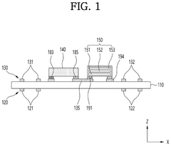
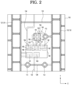
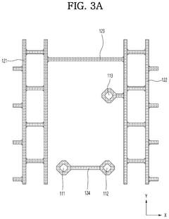
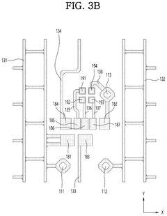
Transparent display device
PatentPendingUS20250268006A1
Innovation
- A transparent display device design where power wirings on different layers are vertically overlapped, with capacitors formed by overlapping power wirings and the substrate, to increase transmission area and reduce noise interference.
Materials Science Innovations
Recent advancements in transparent transistor technology have been significantly driven by breakthroughs in materials science. The development of novel semiconductor materials with enhanced optical transparency and electrical performance has revolutionized the field. Indium gallium zinc oxide (IGZO) has emerged as a leading material, offering superior electron mobility compared to traditional amorphous silicon while maintaining excellent transparency in the visible spectrum. This material has enabled transistors that operate efficiently while allowing over 90% light transmission.
Another significant innovation has been the development of carbon-based materials, particularly graphene and carbon nanotubes (CNTs). These materials offer exceptional electrical properties with theoretical electron mobilities exceeding 200,000 cm²/Vs, far surpassing conventional semiconductors. Their atomic thickness also contributes to near-perfect transparency, making them ideal candidates for next-generation transparent electronics.
Metal oxide semiconductors beyond IGZO have also shown promising results. Zinc tin oxide (ZTO) and aluminum zinc oxide (AZO) provide cost-effective alternatives with competitive performance metrics. These materials can be deposited using conventional techniques such as sputtering and solution processing, facilitating easier integration into existing manufacturing processes.
Innovative substrate materials have equally contributed to efficiency improvements. The development of flexible transparent substrates, including polyimide derivatives and specialized glass compositions, has enabled transistors that maintain performance under mechanical stress. These substrates feature enhanced thermal stability and reduced surface roughness, addressing key challenges in device fabrication.
Interface engineering represents another crucial innovation area. Novel dielectric materials with high-k properties, such as hafnium oxide and aluminum oxide, have improved gate control efficiency while maintaining transparency. Additionally, specialized surface treatments and buffer layers have reduced interface trap densities, minimizing performance degradation over time.
Nanomaterial composites combining different transparent conductors have emerged as a promising approach. These hybrid materials leverage the complementary properties of their components, such as the high conductivity of silver nanowires combined with the mechanical stability of metal oxides, resulting in transparent electrodes with optimized performance characteristics.
Processing innovations have equally advanced the field. Low-temperature deposition techniques, including solution processing and atomic layer deposition, have enabled the fabrication of high-performance transparent transistors on temperature-sensitive substrates. These methods have expanded application possibilities while reducing manufacturing energy requirements and associated costs.
Sustainability and Manufacturing Scalability
The sustainability and manufacturing scalability of transparent transistors represent critical factors in their commercial viability and environmental impact. Current manufacturing processes for transparent transistors often involve energy-intensive deposition techniques and rare materials, creating challenges for large-scale production. Metal oxide-based transparent transistors, particularly those using indium gallium zinc oxide (IGZO), demonstrate superior sustainability profiles compared to alternatives, with lower processing temperatures and reduced energy consumption during fabrication.
Environmental considerations reveal significant differences between competing technologies. While amorphous silicon requires high-temperature processing exceeding 300°C, oxide semiconductors can be manufactured at temperatures below 200°C, resulting in approximately 40% energy savings. Additionally, the stability of oxide-based transistors extends device lifespans, reducing electronic waste generation. However, the reliance on indium—a scarce element—presents supply chain vulnerabilities that must be addressed through material innovation or recycling initiatives.
Manufacturing scalability varies considerably across transparent transistor technologies. Solution-processed organic transistors offer cost advantages and compatibility with roll-to-roll processing but suffer from lower performance metrics and stability issues. In contrast, vacuum-deposited oxide transistors provide superior electrical characteristics while requiring more capital-intensive equipment. Recent advancements in spatial atomic layer deposition (SALD) techniques have demonstrated promising results for high-throughput manufacturing of high-quality oxide semiconductor layers at atmospheric pressure.
Economic analysis indicates that while initial capital expenditure for oxide transistor production lines exceeds that of conventional silicon-based facilities, the operational costs trend lower over time due to reduced material waste and energy consumption. Industry projections suggest that economies of scale could reduce manufacturing costs by 30-45% within five years as production volumes increase and process optimizations mature.
The circular economy potential of transparent transistor technologies varies significantly. Carbon-based alternatives offer biodegradability advantages but with performance trade-offs, while metal oxide systems present better recyclability of substrate materials. Emerging research into bio-derived transparent conductors and semiconductors shows promise for reducing the environmental footprint of next-generation devices, though commercial viability remains several years away.
For sustainable scaling, manufacturers must balance performance requirements with environmental considerations through material selection optimization, process efficiency improvements, and end-of-life management strategies. The industry trend toward thinner films and lower processing temperatures aligns with both sustainability goals and cost reduction imperatives, creating a positive trajectory for future development.
Unlock deeper insights with PatSnap Eureka Quick Research — get a full tech report to explore trends and direct your research. Try now!
Generate Your Research Report Instantly with AI Agent
Supercharge your innovation with PatSnap Eureka AI Agent Platform!