Transparent Transistors in Flexible Display Manufacturing
OCT 21, 202510 MIN READ
Generate Your Research Report Instantly with AI Agent
Patsnap Eureka helps you evaluate technical feasibility & market potential.
Transparent Transistor Technology Evolution and Objectives
Transparent transistors have emerged as a critical enabling technology for flexible display manufacturing, evolving significantly since their inception in the early 2000s. Initially developed using amorphous oxide semiconductors, these transistors represented a paradigm shift from traditional silicon-based technologies. The fundamental breakthrough came with the discovery that certain metal oxides, particularly those containing indium, gallium, and zinc (IGZO), could maintain reasonable electron mobility while remaining optically transparent, addressing a long-standing challenge in display technology.
The evolution of transparent transistor technology has followed a trajectory marked by continuous improvements in performance metrics. Early iterations suffered from stability issues, particularly under environmental stress conditions such as temperature fluctuations and humidity. Subsequent research focused on enhancing carrier mobility, reducing threshold voltage, and improving operational stability through materials engineering and novel device architectures. The field has progressed from basic proof-of-concept devices with mobilities below 1 cm²/Vs to advanced systems achieving values exceeding 50 cm²/Vs while maintaining transparency above 80% in the visible spectrum.
A significant milestone in this evolution was the transition from rigid to flexible substrates, enabling the development of bendable and rollable displays. This transition necessitated innovations in low-temperature processing techniques, as traditional high-temperature annealing methods were incompatible with polymer substrates. Solution-processing routes emerged as promising alternatives, offering cost-effective manufacturing while maintaining essential performance characteristics.
The primary objective of current research is to develop transparent transistor technologies that simultaneously satisfy multiple requirements: high optical transparency, excellent electrical performance, mechanical flexibility, environmental stability, and compatibility with large-area, low-cost manufacturing processes. Specifically, researchers aim to achieve electron mobilities exceeding 30 cm²/Vs, optical transparency above 90%, and operational stability over 10,000 bending cycles at radii below 1 mm.
Future objectives include the development of stretchable transparent transistors capable of withstanding not only bending but also tensile strain exceeding 20% without performance degradation. Additionally, there is growing interest in developing transparent transistors with tunable bandgaps to enable multifunctional devices that can serve as both active matrix elements and photodetectors in next-generation display systems. The ultimate goal is to create fully transparent, flexible electronic systems that can be manufactured using roll-to-roll processes, dramatically reducing production costs while enabling novel form factors and applications.
Market Analysis for Flexible Display Applications
The flexible display market has witnessed remarkable growth in recent years, driven by increasing consumer demand for portable, lightweight, and durable electronic devices. The global flexible display market was valued at approximately $23.1 billion in 2022 and is projected to reach $42.5 billion by 2027, growing at a CAGR of 13.0% during the forecast period. This substantial growth trajectory underscores the significant market potential for transparent transistor technologies in flexible display manufacturing.
Consumer electronics represents the largest application segment for flexible displays, accounting for over 60% of the market share. Smartphones and wearable devices are the primary drivers within this segment, with major manufacturers like Samsung, Apple, and Huawei increasingly incorporating flexible display technologies into their flagship products. The automotive industry is emerging as another promising application area, with a projected CAGR of 15.2% through 2027, as vehicle manufacturers integrate flexible displays into dashboard systems and entertainment consoles.
Geographically, Asia-Pacific dominates the flexible display market, holding approximately 45% of the global market share. This regional dominance is attributed to the presence of major display manufacturers and electronic device producers in countries like South Korea, Japan, China, and Taiwan. North America and Europe follow with market shares of 28% and 20% respectively, primarily driven by high consumer adoption rates of premium electronic devices featuring flexible displays.
The integration of transparent transistors in flexible display manufacturing addresses several critical market needs. First, it enables the production of truly transparent displays with transparency rates exceeding 80%, opening new application possibilities in augmented reality, smart windows, and automotive heads-up displays. Second, it facilitates the development of ultra-thin and lightweight displays, meeting consumer preferences for portable devices. Third, transparent transistors contribute to reduced power consumption, addressing battery life concerns in mobile devices.
Market research indicates that consumers are willing to pay a premium of 15-20% for devices featuring advanced flexible display technologies, particularly those offering enhanced durability, better visual performance, and novel form factors. This price elasticity provides manufacturers with sufficient margin to invest in transparent transistor technologies despite their currently higher production costs.
Industry analysts forecast that the market penetration of transparent transistor-based flexible displays will reach 25% of the total flexible display market by 2028, representing a significant opportunity for early adopters of this technology. The healthcare, retail, and defense sectors are identified as emerging application areas with high growth potential, particularly for transparent display solutions that can be integrated into existing infrastructure or equipment.
Current Limitations and Technical Barriers in Transparent Electronics
Despite significant advancements in transparent electronics, several critical limitations and technical barriers continue to impede the widespread implementation of transparent transistors in flexible display manufacturing. The most fundamental challenge remains the inherent trade-off between optical transparency and electrical performance. As transparency increases, carrier mobility and conductivity typically decrease, creating a persistent engineering dilemma that requires sophisticated material design and device architecture.
Material limitations represent another significant barrier. Conventional transparent conducting oxides (TCOs) like indium tin oxide (ITO) exhibit brittleness that contradicts the flexibility requirements of next-generation displays. When subjected to repeated bending, these materials develop microcracks that dramatically increase resistance and eventually lead to device failure. This mechanical instability severely restricts their application in truly flexible or rollable displays.
Processing temperature compatibility presents a substantial technical hurdle. High-quality transparent oxide semiconductors traditionally require high-temperature annealing (>300°C) to achieve optimal electrical properties and stability. However, flexible substrates like polyimide or PET typically cannot withstand temperatures above 200°C without deformation, creating a fundamental process incompatibility that necessitates the development of low-temperature fabrication techniques.
Stability issues further complicate transparent transistor implementation. Transparent oxide semiconductors, particularly amorphous oxide semiconductors (AOS), often exhibit threshold voltage shifts under prolonged bias stress or illumination. This bias stress instability results in inconsistent pixel driving in displays, causing image retention or "burn-in" effects that significantly reduce device lifetime and reliability.
Interface engineering challenges also persist at the semiconductor-dielectric interface. Poor interface quality leads to charge trapping, carrier scattering, and ultimately degraded device performance. The development of compatible dielectric materials that form high-quality interfaces with transparent semiconductors while maintaining transparency and flexibility remains technically demanding.
Uniformity and scalability issues present manufacturing barriers. Achieving consistent electrical properties across large-area substrates is particularly challenging for transparent semiconductors. Variations in film thickness, composition, and microstructure lead to non-uniform device performance across display panels, resulting in yield losses during mass production.
Finally, environmental sensitivity poses reliability concerns. Many transparent semiconductor materials, particularly zinc oxide-based compounds, demonstrate sensitivity to ambient conditions including humidity, oxygen, and light exposure. This environmental instability necessitates complex encapsulation solutions that add cost and complexity while potentially reducing overall transparency and flexibility.
Current Fabrication Methods for Transparent Transistors
01 Transparent oxide semiconductor materials for transistors
Transparent transistors can be fabricated using oxide semiconductor materials such as indium gallium zinc oxide (IGZO), zinc oxide (ZnO), or tin oxide (SnO2). These materials offer high electron mobility while maintaining optical transparency in the visible spectrum. The use of these oxide semiconductors enables the creation of transistors that can be integrated into transparent electronic devices without compromising visibility or display quality.- Transparent oxide semiconductor materials for transistors: Various oxide semiconductor materials can be used to create transparent transistors. These materials, such as indium gallium zinc oxide (IGZO), zinc oxide (ZnO), and other metal oxides, offer high optical transparency while maintaining good electrical properties. The transparency of these materials allows for the development of fully transparent electronic devices that can be integrated into displays, windows, and other transparent surfaces.
- Transparent electrode materials and structures: Transparent electrodes are essential components of transparent transistors. Materials such as indium tin oxide (ITO), graphene, silver nanowires, and other conductive transparent materials are used to create the gate, source, and drain electrodes of transparent transistors. The structure and composition of these electrodes significantly impact the overall transparency and performance of the transistor devices.
- Transparent substrate technologies: Transparent substrates serve as the foundation for transparent transistors. Materials such as glass, flexible polymers, and other transparent materials are used as substrates. The choice of substrate affects not only the optical transparency but also the mechanical properties, thermal stability, and compatibility with various fabrication processes. Advanced substrate technologies enable the development of flexible and bendable transparent transistor devices.
- Transparency enhancement techniques: Various techniques are employed to enhance the transparency of transistors. These include optimizing layer thicknesses, using anti-reflection coatings, implementing novel device architectures, and developing specialized fabrication processes. These techniques aim to minimize light absorption and scattering, thereby maximizing the optical transparency while maintaining or improving the electrical performance of the transistors.
- Applications of transparent transistors: Transparent transistors find applications in various fields including transparent displays, smart windows, augmented reality devices, and transparent electronics. The ability to create fully transparent electronic circuits enables the development of innovative products where visibility through the device is required. These applications leverage the unique combination of optical transparency and electronic functionality offered by transparent transistors.
02 Transparent electrode materials and structures
Transparent electrodes are essential components of transparent transistors, typically made from materials like indium tin oxide (ITO), fluorine-doped tin oxide (FTO), or graphene. These electrodes need to balance electrical conductivity with optical transparency. Advanced structures such as mesh electrodes, nanowire networks, or ultrathin metal films can be employed to optimize both properties, allowing for efficient charge transport while maintaining high transparency levels in the final transistor device.Expand Specific Solutions03 Fabrication techniques for transparent transistors
Various fabrication methods are employed to create transparent transistors, including solution processing, vacuum deposition, and printing techniques. Low-temperature processes are particularly valuable as they allow deposition on temperature-sensitive transparent substrates like plastic. Advanced patterning techniques such as photolithography, inkjet printing, or laser patterning help define the transistor structures while maintaining transparency. These fabrication approaches enable the mass production of transparent transistors for various applications.Expand Specific Solutions04 Integration of transparent transistors in display technologies
Transparent transistors are crucial components in advanced display technologies, enabling the creation of transparent displays, heads-up displays, and augmented reality devices. When integrated into display backplanes, these transistors control individual pixels while remaining invisible to the user. The transparency of these transistors allows for novel display designs such as see-through displays, dual-sided displays, or displays that can be integrated into windows or windshields, enhancing user experience and enabling new applications.Expand Specific Solutions05 Enhancement of transparency and performance optimization
Various techniques are employed to enhance the transparency and performance of transistors, including the use of anti-reflection coatings, optimization of layer thicknesses, and careful material selection. Balancing the trade-off between transparency and electrical performance often requires innovative device architectures and material combinations. Additionally, encapsulation layers that protect the transistors while maintaining transparency are essential for long-term stability and reliability in various environmental conditions.Expand Specific Solutions
Leading Companies and Research Institutions in Flexible Display
The transparent transistor market in flexible display manufacturing is currently in a growth phase, with increasing demand driven by the expanding flexible electronics sector. Market size is projected to grow significantly as applications in wearable devices, foldable smartphones, and automotive displays gain traction. Technologically, the field is advancing rapidly with key players at different maturity levels. Japanese entities (Japan Science & Technology Agency, Semiconductor Energy Laboratory, Tokyo Institute of Technology) and Korean companies (Samsung Display) lead in innovation, while Chinese manufacturers (BOE Technology, China Star Optoelectronics) focus on scaling production. Western institutions (Purdue Research Foundation, Northwestern University) contribute fundamental research. Companies like Canon, Sharp, and Seiko Epson are developing specialized applications, indicating the technology is transitioning from research to commercial implementation across global markets.
Semiconductor Energy Laboratory Co., Ltd.
Technical Solution: Semiconductor Energy Laboratory (SEL) has pioneered oxide semiconductor technology for transparent transistors, particularly focusing on IGZO (Indium Gallium Zinc Oxide) thin-film transistors. Their approach involves creating highly uniform amorphous IGZO films with optimized oxygen vacancy concentration to achieve both transparency and high electron mobility (typically 10-15 cm²/Vs)[1]. SEL has developed proprietary deposition techniques that enable low-temperature processing (below 300°C), making their technology compatible with flexible substrates like polyimide films. Their transistors maintain over 80% optical transparency in the visible spectrum while achieving switching speeds sufficient for high-resolution displays[3]. SEL has also addressed stability issues through passivation layers and specialized annealing processes that reduce threshold voltage shifts during prolonged operation. Their technology enables backplane integration in flexible displays with bending radii below 5mm while maintaining electrical performance[5].
Strengths: Industry-leading expertise in oxide semiconductor physics; extensive patent portfolio; proven manufacturing scalability; compatibility with existing display production infrastructure. Weaknesses: Higher production costs compared to conventional silicon-based technologies; requires specialized deposition equipment; some remaining challenges with long-term stability under extreme bending conditions.
BOE Technology Group Co., Ltd.
Technical Solution: BOE has developed a comprehensive transparent transistor technology platform specifically for flexible OLED displays. Their approach centers on low-temperature polysilicon oxide (LTPO) backplanes that combine oxide TFTs for static display areas with LTPS (Low-Temperature Polysilicon) TFTs for high-frequency driving circuits[2]. BOE's manufacturing process utilizes specialized sputtering techniques with precise oxygen partial pressure control to create highly uniform metal oxide semiconductor layers. Their transistors achieve transparency exceeding 85% in the visible spectrum while maintaining electron mobility of 5-12 cm²/Vs[4]. For flexible applications, BOE employs a proprietary neutral plane engineering approach where the transistor array is positioned at the mechanical neutral plane of the device stack, minimizing strain during bending. This allows their displays to achieve bending radii below 3mm without significant performance degradation[6]. BOE has also pioneered in-cell touch integration with their transparent transistor arrays, reducing overall display thickness.
Strengths: Vertical integration from materials to finished displays; massive production capacity; advanced process control systems; strong position in both OLED and LCD applications. Weaknesses: Relatively higher defect rates in flexible applications compared to rigid displays; challenges with yield consistency across large substrate sizes; some limitations in extreme environmental conditions.
Key Patents and Scientific Breakthroughs in Transparent Electronics
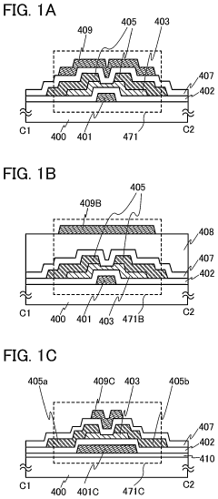
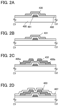
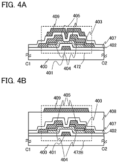
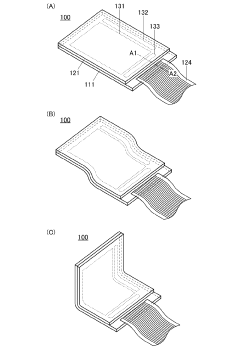
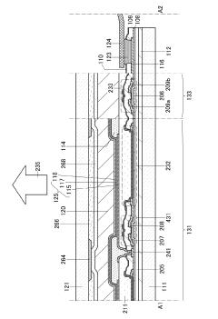
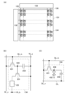
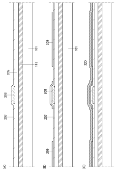
Display device including transistor and manufacturing method thereof
PatentActiveUS20240234432A1
Innovation
- A display device is developed with a transistor featuring an oxide semiconductor layer that undergoes heat treatment for dehydration or dehydrogenation, followed by the application of a protective insulating layer made from inorganic materials containing oxygen, which helps stabilize the carrier concentration and reduce impurities, thereby enhancing the transistor's reliability and electric characteristics.
Display device
PatentInactiveJP2023182716A
Innovation
- Integration of translucent semiconductor film in transistors on a flexible substrate, enabling high flexibility while maintaining display functionality.
- Unique capacitive element design where the first insulator film does not cover the region where the first electrode contacts the dielectric film, potentially improving capacitive response.
- Structural arrangement that combines flexible substrate with translucent components to achieve a highly flexible display device.
Material Science Advancements for Transparent Conductive Films
The evolution of transparent conductive films (TCFs) represents a cornerstone advancement in flexible display manufacturing, particularly for transparent transistor applications. Traditional indium tin oxide (ITO) has dominated the market for decades due to its excellent combination of optical transparency and electrical conductivity. However, ITO's inherent brittleness and limited flexibility have prompted intensive research into alternative materials that can better accommodate the mechanical requirements of flexible displays.
Recent breakthroughs in nanomaterials have yielded promising alternatives to ITO. Carbon-based materials, particularly graphene and carbon nanotubes (CNTs), demonstrate exceptional mechanical flexibility while maintaining high electrical conductivity. Single-layer graphene exhibits transparency exceeding 97% with sheet resistance as low as 30 Ω/sq when doped appropriately. Meanwhile, CNT networks can achieve transparency of 90% with comparable conductivity metrics while offering superior bending durability.
Metal nanowire networks, especially those based on silver (AgNWs), have emerged as another viable alternative. These networks can achieve transparency above 90% with sheet resistance below 10 Ω/sq. The interconnected mesh structure of AgNWs provides resilience to mechanical deformation, with some formulations maintaining performance even after thousands of bending cycles at radii below 5mm.
Hybrid structures combining multiple materials represent the cutting edge of TCF development. PEDOT:PSS polymer composites enhanced with metal nanowires or graphene demonstrate synergistic improvements in both conductivity and mechanical properties. These hybrids address the limitations of individual materials while capitalizing on their respective strengths.
Atomic layer deposition (ALD) techniques have revolutionized the fabrication of ultra-thin metal oxide films, enabling precise control over thickness and composition. This has led to the development of amorphous oxide semiconductors like IGZO (indium gallium zinc oxide) with unprecedented uniformity and performance characteristics for transparent transistor applications.
Solution-processing methods have gained significant attention for their compatibility with roll-to-roll manufacturing processes. These approaches substantially reduce production costs while enabling large-area fabrication essential for commercial-scale flexible displays. Advances in solution chemistry have addressed previous limitations regarding film uniformity and electrical performance.
The environmental stability of TCFs remains a critical challenge, particularly for organic and nanomaterial-based films. Recent developments in encapsulation technologies and intrinsic material modifications have significantly improved resistance to oxygen and moisture degradation, extending operational lifetimes from months to several years under normal conditions.
Sustainability and Environmental Impact of Flexible Display Manufacturing
The environmental impact of flexible display manufacturing, particularly those incorporating transparent transistors, presents significant sustainability challenges and opportunities. Traditional display manufacturing processes are resource-intensive and generate substantial waste, with high energy consumption and hazardous chemical usage. The transition to flexible displays introduces new environmental considerations that must be addressed through comprehensive lifecycle assessment.
Material selection represents a critical factor in sustainable flexible display production. Conventional transparent transistors often utilize indium tin oxide (ITO), which faces supply constraints and extraction-related environmental degradation. Alternative materials such as graphene, carbon nanotubes, and metal nanowires offer promising sustainability advantages, including reduced rare earth mineral dependence and potentially lower environmental footprints when properly implemented.
Energy consumption during manufacturing remains a significant concern, with clean room operations and high-temperature processes contributing substantially to carbon emissions. Recent innovations in low-temperature processing for transparent transistor fabrication show promise for reducing energy requirements by 30-45% compared to traditional methods, representing a meaningful advancement toward sustainability goals.
Chemical usage presents another environmental challenge, as etching processes and cleaning agents often involve hazardous substances. Solution-based deposition techniques for transparent transistor layers can reduce chemical waste by up to 60% while minimizing worker exposure to harmful compounds. Additionally, emerging water-based processing methods demonstrate potential for further reducing environmental impact through decreased solvent usage.
End-of-life considerations are increasingly important as flexible display adoption accelerates. The complex material integration in these displays, including transparent transistor components, creates recycling challenges that current infrastructure struggles to address. Design-for-disassembly approaches and modular construction methods are being explored to facilitate material recovery and component reuse, potentially extending product lifecycles and reducing electronic waste.
Regulatory frameworks worldwide are evolving to address these environmental concerns, with the European Union's Restriction of Hazardous Substances (RoHS) and Registration, Evaluation, Authorization and Restriction of Chemicals (REACH) regulations significantly influencing manufacturing practices. Companies developing transparent transistor technologies for flexible displays must navigate these requirements while balancing performance objectives with sustainability goals.
Industry initiatives focused on green chemistry principles and circular economy approaches are gaining momentum, with several major manufacturers committing to carbon-neutral production timelines. These efforts include renewable energy integration, closed-loop water systems, and advanced waste treatment technologies specifically designed for flexible electronics manufacturing facilities.
Unlock deeper insights with Patsnap Eureka Quick Research — get a full tech report to explore trends and direct your research. Try now!
Generate Your Research Report Instantly with AI Agent
Supercharge your innovation with Patsnap Eureka AI Agent Platform!