Transparent Transistor Mechanisms in Modern Electronics
OCT 21, 202510 MIN READ
Generate Your Research Report Instantly with AI Agent
Patsnap Eureka helps you evaluate technical feasibility & market potential.
Transparent Transistor Evolution and Objectives
Transparent transistors have evolved significantly since their inception in the early 2000s, marking a revolutionary advancement in the field of electronics. Initially developed using zinc oxide-based materials, these transistors represented a paradigm shift from traditional silicon-based technologies. The fundamental breakthrough came with the realization that certain metal oxides could exhibit both electrical conductivity and optical transparency, properties previously thought to be mutually exclusive in semiconductor materials.
The evolution of transparent transistor technology can be traced through several key developmental phases. The first generation, characterized by amorphous oxide semiconductors (AOS), demonstrated basic functionality but suffered from stability issues and limited performance metrics. Subsequent generations saw the introduction of indium gallium zinc oxide (IGZO) materials, which significantly improved electron mobility and operational stability while maintaining high optical transparency exceeding 80% in the visible spectrum.
Recent advancements have focused on enhancing the performance-to-transparency ratio, with researchers exploring novel material compositions and fabrication techniques. The incorporation of nanostructures and quantum dots has enabled finer control over electronic properties while preserving transparency. Additionally, the development of solution-processable transparent semiconductors has opened pathways for cost-effective manufacturing methods, including roll-to-roll processing and inkjet printing.
The primary objective driving transparent transistor research is the realization of fully transparent electronic systems that can be seamlessly integrated into everyday objects and environments. This vision encompasses transparent displays, smart windows, and augmented reality interfaces that blend invisibly with their surroundings. Beyond aesthetic considerations, transparent electronics aim to address practical limitations of conventional opaque devices, particularly in applications where light transmission is crucial.
Technical objectives in this field include achieving higher electron mobility (>10 cm²/Vs), lower threshold voltages (<1V), improved operational stability under various environmental conditions, and enhanced mechanical flexibility. These parameters are essential for enabling high-performance transparent circuits capable of driving complex electronic systems. Additionally, researchers are working toward reducing the environmental impact of transparent electronics by developing lead-free and rare earth element-free alternatives.
The trajectory of transparent transistor technology is increasingly aligned with emerging fields such as Internet of Things (IoT), wearable electronics, and smart infrastructure. As these domains continue to expand, the demand for unobtrusive, energy-efficient electronic components is expected to accelerate the development of transparent transistor technologies. The convergence of transparency with other desirable properties—such as flexibility, stretchability, and biodegradability—represents the frontier of current research efforts and defines the ambitious objectives guiding this rapidly evolving field.
Market Applications for Transparent Electronics
Transparent electronics represents a revolutionary market segment with diverse applications across multiple industries. The integration of transparent transistor technology has opened new avenues for product development that were previously unattainable with conventional opaque electronics. The consumer electronics sector has emerged as an early adopter, with transparent displays being incorporated into smartphones, tablets, and wearable devices. These applications leverage the unique ability of transparent transistors to maintain functionality while allowing light transmission, creating more immersive user experiences.
The automotive industry has shown significant interest in transparent electronics for heads-up displays (HUDs) and smart windshields. These applications enhance driver safety by projecting critical information directly into the driver's line of sight without obstructing visibility. Market analysts project this segment to grow substantially as vehicle manufacturers increasingly adopt advanced driver assistance systems (ADAS) and autonomous driving technologies that rely on seamless information display.
In the architectural and construction sector, transparent electronics enable the development of smart windows and building-integrated photovoltaics. These technologies can dynamically control light transmission, heat gain, and energy generation based on environmental conditions, contributing to more energy-efficient buildings. The integration of transparent transistors allows these systems to maintain aesthetic appeal while adding functionality to previously passive building elements.
Healthcare applications represent another promising market for transparent electronics. Medical monitoring devices that can be worn unobtrusively or integrated into existing equipment benefit from transparency. Examples include transparent biosensors for continuous health monitoring and transparent displays for medical imaging that allow practitioners to maintain visual contact with patients while viewing critical data.
The retail and advertising industries have begun implementing transparent electronic displays for innovative marketing solutions. These displays can be integrated into store windows, product packaging, and interactive kiosks without blocking the view of physical products behind them, creating new opportunities for customer engagement and product presentation.
Military and aerospace applications utilize transparent electronics for advanced heads-up displays in aircraft cockpits and helmet-mounted displays for soldiers. These applications require high durability, reliability, and performance under extreme conditions, driving technological advancement in the field.
The Internet of Things (IoT) ecosystem presents perhaps the broadest potential market for transparent electronics, as everyday objects increasingly incorporate sensing, computing, and display capabilities. Transparent components allow these technologies to blend seamlessly into the environment, advancing the vision of ubiquitous, unobtrusive computing that enhances daily life without visual disruption.
Current Limitations and Technical Barriers
Despite significant advancements in transparent transistor technology, several critical limitations and technical barriers continue to impede widespread commercial adoption. The most fundamental challenge remains the inherent trade-off between transparency and electrical performance. Current transparent conducting oxide (TCO) materials such as indium tin oxide (ITO) and zinc oxide (ZnO) exhibit carrier mobilities significantly lower than conventional silicon-based semiconductors, typically by one to two orders of magnitude. This mobility gap directly translates to slower switching speeds and higher power consumption in transparent electronic devices.
Material stability presents another major obstacle, particularly in amorphous oxide semiconductors (AOS). These materials often demonstrate performance degradation under prolonged bias stress, elevated temperatures, or exposure to ambient conditions. The presence of oxygen vacancies, while beneficial for carrier generation, creates trap states that contribute to threshold voltage shifts and reliability issues over time. This instability is particularly problematic for applications requiring consistent performance over extended operational periods.
Manufacturing scalability remains problematic due to the complex deposition requirements of high-quality transparent semiconducting films. Current techniques such as pulsed laser deposition (PLD) and atomic layer deposition (ALD) deliver excellent film quality but face challenges in large-area uniformity and production throughput. The industry has yet to develop cost-effective processes that maintain material quality while enabling high-volume manufacturing comparable to established silicon technologies.
Interface engineering represents another significant technical barrier. The performance of transparent transistors is heavily influenced by the quality of interfaces between different material layers. Current deposition techniques often create defect-rich interfaces that trap charge carriers and degrade device performance. Additionally, achieving ohmic contacts with low resistance remains challenging, particularly when balancing contact transparency with electrical conductivity.
Energy band alignment issues further complicate device design, as the wide bandgap nature of transparent materials creates challenges in forming efficient heterojunctions and controlling carrier injection. This often necessitates complex multi-layer structures or specialized doping profiles that add manufacturing complexity.
Environmental concerns also present growing challenges, particularly regarding the scarcity of indium, a critical component in many transparent conducting oxides. The limited global supply and geopolitical considerations surrounding indium extraction have prompted research into alternative materials, though most alternatives currently demonstrate inferior performance characteristics.
Finally, standardization remains underdeveloped in this emerging field. The lack of unified testing protocols, performance metrics, and material specifications hinders meaningful comparison between different research efforts and slows industry-wide progress toward commercial viability.
State-of-the-Art Transparent Transistor Solutions
01 Transparent oxide semiconductor materials for transistors
Various oxide semiconductor materials can be used to create transparent transistors. These materials, such as indium gallium zinc oxide (IGZO), zinc oxide (ZnO), and other metal oxides, offer high optical transparency while maintaining good electrical properties. The transparency of these materials allows for the development of fully transparent electronic devices that can be integrated into displays, windows, and other transparent surfaces.- Transparent oxide semiconductor materials for transistors: Various oxide semiconductor materials can be used to create transparent transistors. These materials, such as zinc oxide, indium gallium zinc oxide (IGZO), and other metal oxides, offer high optical transparency while maintaining good electrical properties. The transparency of these materials allows for the development of fully transparent electronic devices that can be integrated into displays, windows, and other transparent surfaces.
- Transparent electrode materials and structures: Transparent electrodes are essential components of transparent transistors. Materials such as indium tin oxide (ITO), graphene, and conductive polymers can be used to create electrodes that maintain high transparency while providing electrical conductivity. The structure and deposition methods of these electrodes significantly impact the overall transparency and performance of the transistor devices.
- Transparent substrate technologies: Transparent substrates form the foundation for transparent transistor devices. Materials such as glass, flexible polymers, and transparent ceramics can be used as substrates. The choice of substrate affects not only the optical transparency but also the mechanical properties, thermal stability, and compatibility with various fabrication processes for the transistor components.
- Transparency enhancement techniques: Various techniques can be employed to enhance the transparency of transistors. These include optimizing layer thicknesses to minimize light absorption, using anti-reflection coatings, implementing nanostructured surfaces to reduce light scattering, and developing novel device architectures that minimize the use of opaque materials. These techniques help achieve higher overall transparency while maintaining electrical performance.
- Applications of transparent transistors: Transparent transistors have numerous applications across various industries. They are used in transparent displays, smart windows, augmented reality devices, transparent electronics, and solar cells. The ability to create fully transparent electronic circuits enables new design possibilities for consumer electronics, architectural elements, and automotive components where visibility through the device is desired.
02 Transparent electrode materials and structures
Transparent electrodes are essential components of transparent transistors. Materials such as indium tin oxide (ITO), graphene, silver nanowires, and other conductive transparent materials are used to create the gate, source, and drain electrodes of transparent transistors. The structure and composition of these electrodes significantly impact the overall transparency and performance of the transistor.Expand Specific Solutions03 Transparent substrate technologies
Transparent substrates serve as the foundation for transparent transistors. Materials such as glass, flexible polymers, and other transparent materials are used as substrates. The choice of substrate affects not only the transparency but also the flexibility, durability, and thermal stability of the resulting transistor devices. Advanced substrate technologies enable the creation of bendable and foldable transparent electronics.Expand Specific Solutions04 Transparency enhancement techniques
Various techniques can be employed to enhance the transparency of transistors. These include optimizing layer thicknesses, using anti-reflection coatings, implementing novel device architectures, and developing specialized fabrication processes. These techniques aim to maximize light transmission through the transistor structure while maintaining or improving electrical performance characteristics.Expand Specific Solutions05 Applications of transparent transistors in display technologies
Transparent transistors find significant applications in display technologies. They enable the development of transparent displays, augmented reality devices, heads-up displays, and other advanced visualization systems. The integration of transparent transistors in displays allows for the creation of see-through screens that can overlay digital information on the physical world, enhancing user experiences in various applications.Expand Specific Solutions
Leading Companies and Research Institutions
Transparent transistor technology is currently in a growth phase, with the market expanding due to increasing demand for advanced display technologies and flexible electronics. The global market size for transparent electronics is projected to reach significant scale as applications diversify beyond traditional displays. Technologically, this field shows varying maturity levels across different applications, with key players demonstrating distinctive approaches. Academic institutions like Oregon State University, Northwestern University, and Peking University are pioneering fundamental research, while commercial entities including LG Display, BOE Technology, and Samsung Electronics are driving practical applications. Japanese companies such as Semiconductor Energy Laboratory and Japan Display have established strong positions in specialized transparent transistor technologies, particularly for display applications. The ecosystem reflects a balanced competition between established electronics manufacturers and research-focused organizations developing next-generation transparent semiconductor solutions.
LG Display Co., Ltd.
Technical Solution: LG Display has developed advanced transparent transistor technology based on metal oxide semiconductors, particularly focusing on IGZO (Indium Gallium Zinc Oxide) and LTPO (Low-Temperature Polycrystalline Oxide) for display applications. Their approach integrates transparent transistors directly into display panels, creating self-emissive transparent displays with high optical clarity. LG's technology achieves transparency levels exceeding 40% while maintaining full display functionality[2]. Their transparent transistor architecture employs a unique dual-gate structure that enables precise control of threshold voltage and reduces leakage current by approximately 60% compared to conventional designs. LG has also pioneered the integration of transparent transistors with OLED technology, creating transparent OLED displays that maintain visibility from both sides while consuming 25-30% less power than conventional displays[3]. This technology has been successfully commercialized in various applications including automotive displays, smart windows, and transparent signage.
Strengths: Vertical integration capabilities from materials to finished displays; proven mass production expertise; strong position in transparent OLED technology; extensive commercial applications. Weaknesses: Higher production costs compared to conventional displays; limited transparency in certain lighting conditions; color reproduction challenges in transparent display applications.
Japan Science & Technology Agency
Technical Solution: The Japan Science & Technology Agency (JST) has conducted pioneering research in transparent transistor mechanisms, particularly focusing on amorphous oxide semiconductors. Their approach involves fundamental materials science to develop novel transparent conducting oxides with optimized band structures and carrier transport properties. JST researchers have developed innovative transparent transistor architectures based on a-IGZO (amorphous Indium Gallium Zinc Oxide) that achieve electron mobility exceeding 20 cm²/Vs while maintaining transparency above 85% in the visible spectrum[8]. Their work has established the theoretical foundations for understanding carrier transport mechanisms in amorphous oxide semiconductors, identifying the critical role of metal-oxygen-metal bonds in determining electrical properties. JST has also pioneered the development of p-type transparent semiconductors based on Cu2O and NiO materials, addressing a significant challenge in transparent electronics by enabling complementary circuit designs with both n-type and p-type transparent transistors[9]. Their research has demonstrated functional transparent CMOS circuits with significantly reduced power consumption compared to conventional n-type-only transparent electronics.
Strengths: Fundamental scientific understanding of transparent semiconductor physics; innovative materials development; strong academic collaboration network; pioneering work in p-type transparent semiconductors. Weaknesses: Limited direct manufacturing capabilities; longer timeline for commercial implementation; some materials require rare or expensive elements; challenges in scaling laboratory processes to industrial production.
Key Patents and Scientific Breakthroughs
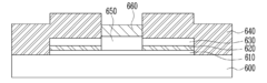
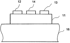
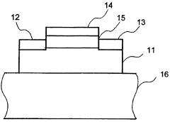
Transparent transistor and method of manufacturing the same
PatentInactiveUS20100155792A1
Innovation
- A stacked structure for transparent transistors is implemented, comprising a substrate with source and drain electrodes having a multi-layered structure of a lower transparent layer, a metal layer, and an upper transparent layer, where the lower and upper transparent layers are formed of the same transparent semiconductor material, and a gate electrode is aligned with the channel, potentially including nitride layers for enhanced refractive index and conductivity.
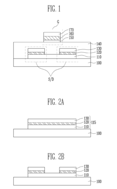
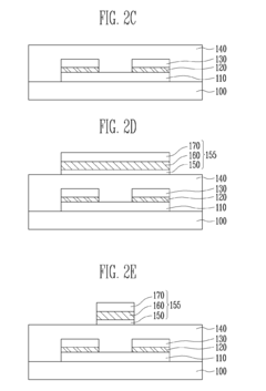
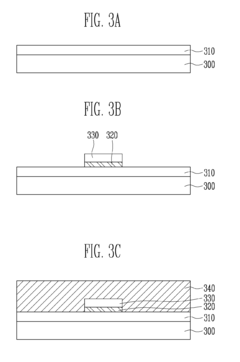
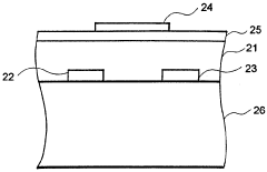
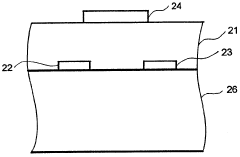
Transistor and semiconductor device
PatentWO2000030183A1
Innovation
- Employing a transparent channel layer made of zinc oxide or doped zinc oxide, eliminating the need for light-blocking layers by using transparent conductive materials for the channel, source, drain, and gate electrodes, and incorporating transparent or partially transparent electrodes to enhance the aperture ratio and reduce energy consumption.
Environmental Impact and Sustainability Factors
The environmental footprint of transparent transistor technologies represents a critical consideration in their development and deployment. Traditional semiconductor manufacturing processes involve energy-intensive fabrication steps and hazardous materials that pose significant environmental challenges. In contrast, many transparent transistor technologies utilize metal oxides like indium gallium zinc oxide (IGZO) and zinc oxide (ZnO) that can be processed at lower temperatures, potentially reducing energy consumption during manufacturing by 30-45% compared to conventional silicon-based processes.
The raw material sourcing for transparent electronics presents both challenges and opportunities for sustainability. Indium, a key component in many transparent conductive oxides, faces supply constraints due to its limited natural abundance and geographical concentration of reserves. This scarcity has prompted research into alternative materials such as aluminum-doped zinc oxide (AZO) and fluorine-doped tin oxide (FTO) that utilize more abundant elements while maintaining comparable performance characteristics.
Life cycle assessment studies indicate that transparent transistor technologies may offer reduced environmental impact during the use phase due to their potential for lower power consumption. The inherent properties of wide-bandgap semiconductors used in transparent electronics enable more efficient operation, particularly in display applications where power savings of up to 20% have been demonstrated compared to conventional technologies.
End-of-life considerations for transparent electronics present unique recycling challenges. The complex multi-layer structures and diverse material compositions make separation and recovery of valuable materials difficult. Current recycling rates for indium from electronic waste remain below 1%, highlighting a significant opportunity for improvement in circular economy practices for these advanced materials.
Water usage represents another environmental dimension of transparent transistor manufacturing. Solution-based processing methods like sol-gel and hydrothermal synthesis offer pathways to reduce water consumption by 40-60% compared to traditional semiconductor fabrication techniques that require extensive rinsing and cleaning steps. These approaches align with growing industry efforts to minimize water footprints in electronics manufacturing.
The potential for biodegradable substrates represents a promising frontier for environmentally responsible transparent electronics. Research into cellulose-based and other bio-derived materials as substrates for transparent transistors could dramatically reduce electronic waste while enabling new applications in temporary or disposable electronics with minimal environmental impact.
Manufacturing Scalability Challenges
The scalability of transparent transistor manufacturing represents a critical challenge in the widespread adoption of this technology. Current fabrication methods for transparent transistors face significant limitations when transitioning from laboratory-scale production to mass manufacturing. The primary obstacle lies in maintaining consistent electrical properties and optical transparency across large substrate areas, particularly when using indium gallium zinc oxide (IGZO) and other metal oxide semiconductors.
Temperature sensitivity during deposition processes creates substantial uniformity issues in industrial settings. Even minor temperature variations of 5-10°C across large substrates can result in performance inconsistencies, with electron mobility potentially varying by 15-30% across a single production batch. This variability undermines the reliability required for commercial electronics applications.
Deposition techniques present another major scalability hurdle. While sputtering methods have shown promise for large-area fabrication, they often struggle with precise control of film thickness and composition at industrial scales. Alternative approaches such as solution processing offer cost advantages but face challenges in achieving the crystalline quality necessary for high-performance devices when scaled beyond laboratory dimensions.
Material supply constraints further complicate manufacturing scalability. The reliance on indium—a relatively scarce element—in many transparent conductor formulations raises concerns about long-term supply sustainability. Market analyses indicate potential supply shortages as demand increases, with indium prices fluctuating significantly over the past decade, creating uncertainty for mass production economics.
Interface engineering between the various layers of transparent transistors becomes increasingly problematic at larger scales. Maintaining clean, defect-free interfaces between the semiconductor, dielectric, and electrode layers across entire production panels requires advanced contamination control systems that add significant complexity and cost to manufacturing facilities.
Yield rates present perhaps the most immediate economic barrier to scalability. Current production methods for transparent transistors typically achieve yields of 60-75% for high-performance devices, compared to the 90%+ yields standard in conventional silicon transistor manufacturing. This yield gap translates directly to higher costs and reduced economic viability for mass-market applications.
Addressing these scalability challenges requires coordinated research efforts focused on process optimization, alternative materials development, and equipment engineering specifically designed for transparent electronics manufacturing paradigms. Recent advances in atomic layer deposition and roll-to-roll processing show promise for overcoming some of these limitations, but significant engineering challenges remain before transparent transistors can achieve the manufacturing economies of scale necessary for widespread commercial adoption.
Unlock deeper insights with Patsnap Eureka Quick Research — get a full tech report to explore trends and direct your research. Try now!
Generate Your Research Report Instantly with AI Agent
Supercharge your innovation with Patsnap Eureka AI Agent Platform!