Transparent Transistor Developments in Augmented Reality Systems
OCT 21, 202510 MIN READ
Generate Your Research Report Instantly with AI Agent
PatSnap Eureka helps you evaluate technical feasibility & market potential.
Transparent Transistor Evolution and AR Integration Goals
Transparent transistors have evolved significantly over the past two decades, transitioning from laboratory curiosities to essential components in advanced display technologies. The journey began with the development of amorphous oxide semiconductors (AOS) in the early 2000s, particularly indium gallium zinc oxide (IGZO), which offered unprecedented combinations of optical transparency and electrical performance. This breakthrough enabled the creation of transistors that could control pixels while remaining invisible to the human eye, a critical requirement for augmented reality (AR) systems where visual clarity is paramount.
The technical evolution has been driven by the increasing demands of AR applications, which require display components that can deliver high resolution, fast response times, and minimal power consumption while maintaining transparency. Early transparent transistor technologies struggled with electron mobility limitations, but recent advancements in materials science have yielded significant improvements, with current-generation transparent transistors achieving mobility values exceeding 10 cm²/Vs—a tenfold improvement over early iterations.
Integration goals for transparent transistors in AR systems focus on several key technical parameters. First, achieving optical transparency exceeding 90% in the visible spectrum while maintaining electrical functionality represents a primary objective. Second, reducing transistor dimensions to accommodate the pixel densities required for high-resolution AR displays (exceeding 2000 PPI) remains a critical challenge. Third, developing manufacturing processes compatible with flexible substrates is essential for next-generation wearable AR devices that conform to facial contours.
The convergence of transparent transistor technology with AR systems aims to overcome the "screen door effect" that has plagued early AR headsets, where visible pixel structures detract from immersion. By integrating truly transparent switching elements, AR display systems can achieve higher pixel densities without compromising the user's view of the real world. This integration also addresses power efficiency concerns, as transparent transistors can be designed to minimize leakage current, extending battery life in portable AR devices.
Looking forward, the technical roadmap for transparent transistors in AR applications includes the development of multi-functional transparent components that combine switching capabilities with sensing functions. This integration would enable AR displays that can adapt to environmental conditions and user interactions without additional opaque components. Research is also focused on enhancing the stability of transparent transistors under various operating conditions, ensuring consistent performance across temperature ranges and extended usage periods.
The ultimate technical goal remains the creation of fully transparent AR display systems that are indistinguishable from conventional eyewear while providing immersive digital overlays. This vision requires continued advancement in transparent transistor technology, particularly in areas of material composition, deposition techniques, and circuit design methodologies tailored to the unique constraints of AR applications.
Market Analysis for AR Display Technologies
The augmented reality (AR) display technology market is experiencing significant growth, driven by increasing adoption across multiple sectors including consumer electronics, healthcare, automotive, and industrial applications. Current market valuations place the global AR display market at approximately $4.2 billion in 2023, with projections indicating a compound annual growth rate (CAGR) of 38% through 2028, potentially reaching $21.5 billion by that time.
Consumer electronics represents the largest segment, accounting for nearly 45% of the market share, with gaming and entertainment applications leading adoption rates. Enterprise applications follow closely, with manufacturing, healthcare, and education showing the most promising growth trajectories.
Geographically, North America dominates the market with approximately 40% share, followed by Asia-Pacific at 35%, which is experiencing the fastest growth due to strong manufacturing capabilities in countries like China, South Korea, and Taiwan. Europe accounts for about 20% of the market, with particular strength in industrial and automotive applications.
The demand for transparent display technologies is primarily driven by the need for more immersive and seamless AR experiences. End-users increasingly expect AR displays with wider fields of view (currently averaging 52 degrees but with market demand pushing toward 90+ degrees), higher resolution (moving from current 1080p toward 4K per eye), and reduced form factors (transitioning from bulky headsets to lightweight glasses).
Market research indicates that transparent transistor technology represents a critical enabler for next-generation AR displays, with 78% of industry professionals identifying display transparency as a key factor limiting mainstream adoption. The integration of transparent transistors could potentially reduce device thickness by up to 40% while increasing light transmission by 25-30%, addressing major consumer pain points.
Competition in this space is intensifying, with major technology companies investing heavily in proprietary display solutions. Recent market entries from Apple, Meta, and Microsoft have established new benchmarks for consumer expectations, while specialized display manufacturers like Samsung Display, LG Display, and BOE Technology are rapidly advancing transparent display capabilities.
Supply chain analysis reveals potential bottlenecks in specialized materials required for transparent transistor production, particularly indium tin oxide alternatives and specialized semiconductor materials, which may impact scaling capabilities in the short term. However, investments in manufacturing infrastructure are accelerating, with over $3.5 billion committed to expanding production capacity for advanced display technologies in the past 18 months.
Current Limitations of Transparent Transistors in AR
Despite significant advancements in transparent transistor technology, several critical limitations continue to impede their optimal implementation in augmented reality (AR) systems. The foremost challenge remains achieving the delicate balance between optical transparency and electrical performance. Current transparent transistors typically exhibit either high transparency with compromised mobility or excellent electrical properties with reduced transparency, creating a fundamental trade-off that limits AR display capabilities.
Material constraints present another significant barrier. Indium gallium zinc oxide (IGZO) and zinc oxide (ZnO) based transistors, while promising, suffer from stability issues under prolonged operation and environmental stressors. The limited availability and rising costs of indium further complicate large-scale production feasibility, raising concerns about sustainable manufacturing for mass-market AR devices.
Manufacturing scalability remains problematic as existing fabrication techniques for transparent transistors often involve complex processes that are difficult to scale while maintaining consistent performance metrics. The precision required for nanoscale features in transparent materials exceeds current industrial capabilities for high-volume production, resulting in low yields and high costs that hinder commercial viability.
Power efficiency represents another critical limitation. Transparent transistors generally consume more power than their silicon counterparts to achieve comparable performance, creating thermal management challenges in the confined spaces of AR headsets and glasses. This inefficiency directly impacts battery life, a crucial consideration for wearable AR systems intended for extended use periods.
Resolution constraints also persist due to the larger feature sizes of transparent transistors compared to conventional silicon technology. This limitation restricts pixel density in transparent displays, affecting the overall visual quality and immersion level of AR experiences. The reduced switching speeds of current transparent transistors further compromise refresh rates and response times essential for seamless AR interactions.
Integration complexity presents additional hurdles as transparent transistors must coexist with other AR system components including sensors, processors, and power management circuits. The interface between transparent and conventional electronics often creates signal degradation and compatibility issues that compromise overall system performance and reliability.
Environmental sensitivity remains a significant concern, with many transparent transistor materials exhibiting performance fluctuations under varying light conditions, temperature changes, and humidity levels. This instability poses particular challenges for AR applications that must function consistently across diverse real-world environments, from bright outdoor settings to dimly lit indoor spaces.
Existing Transparent Transistor Architectures for AR
01 Transparent oxide semiconductor materials for transistors
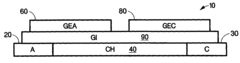
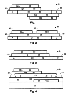
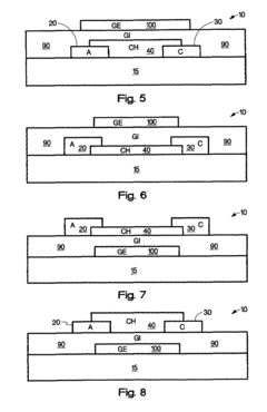
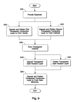
Various oxide semiconductor materials can be used to create transparent transistors. These materials, such as zinc oxide, indium gallium zinc oxide (IGZO), and other metal oxides, offer high optical transparency while maintaining good electrical properties. The use of these materials enables the fabrication of transistors that are visually transparent and can be integrated into displays and other optical devices without blocking light transmission.- Transparent oxide semiconductor materials for transistors: Various oxide semiconductor materials can be used to create transparent transistors. These materials, such as indium gallium zinc oxide (IGZO), zinc oxide (ZnO), and other metal oxides, offer high optical transparency while maintaining good electrical properties. The transparency of these materials allows for the development of fully transparent electronic devices that can be integrated into displays and other applications where visibility through the device is important.
- Transparent electrode materials and structures: Transparent electrodes are essential components of transparent transistors. Materials such as indium tin oxide (ITO), graphene, silver nanowires, and other conductive transparent materials are used to create the gate, source, and drain electrodes of transparent transistors. The structure and composition of these electrodes significantly impact both the electrical performance and optical transparency of the transistor devices.
- Transparent substrate technologies: Transparent transistors require transparent substrates as their foundation. Materials such as glass, flexible polymers like polyethylene terephthalate (PET), and other optically clear materials serve as substrates for transparent transistor fabrication. The choice of substrate affects not only the transparency but also other properties like flexibility, durability, and compatibility with various fabrication processes.
- Fabrication methods for enhancing transparency: Various fabrication techniques are employed to enhance the transparency of transistors. These include thin-film deposition methods, etching processes, and annealing treatments that optimize the optical and electrical properties simultaneously. Advanced patterning techniques allow for minimizing opaque components while maintaining electrical functionality. Post-processing treatments can also improve transparency by reducing defects that cause light scattering.
- Applications of transparent transistors in display technologies: Transparent transistors find significant applications in display technologies. They enable the development of transparent displays, heads-up displays, augmented reality devices, and smart windows. By incorporating transparent transistors, these displays can overlay information on real-world views without blocking visibility. The integration of transparent transistors in active-matrix backplanes allows for high-resolution displays with transparency capabilities.
02 Transparent electrode structures for display applications
Transparent electrodes are crucial components in transparent transistor technology, particularly for display applications. These electrodes, typically made from materials like indium tin oxide (ITO) or other transparent conductive oxides, allow light to pass through while maintaining electrical conductivity. The design and configuration of these electrodes significantly impact the overall transparency and performance of the transistor-based display devices.Expand Specific Solutions03 Fabrication methods for transparent transistor arrays
Various fabrication techniques have been developed to create arrays of transparent transistors. These methods include thin-film deposition processes, photolithography, etching, and annealing treatments that optimize both transparency and electrical performance. Advanced manufacturing approaches enable the creation of uniform transparent transistor arrays on various substrates, including flexible materials, while maintaining high optical clarity and device functionality.Expand Specific Solutions04 Integration of transparent transistors in display technologies
Transparent transistors can be integrated into various display technologies, including LCD, OLED, and emerging display formats. The integration approaches focus on maximizing light transmission while maintaining electrical performance. These transistors serve as switching or driving elements in display pixels without blocking the light path, enabling higher brightness, better efficiency, and novel form factors such as transparent displays and augmented reality devices.Expand Specific Solutions05 Transparency enhancement techniques for transistor components
Various techniques have been developed to enhance the transparency of transistor components. These include optimizing layer thicknesses, using alternative transparent materials for interconnects and insulators, and developing specialized optical coatings. Additional approaches involve structural modifications to minimize light scattering and absorption, resulting in transistors with improved overall transparency while maintaining their electrical functionality.Expand Specific Solutions
Leading Companies in Transparent Transistor Development
Transparent transistor technology in augmented reality systems is currently in a growth phase, with the market expanding rapidly due to increasing demand for AR applications. The global market is projected to reach significant scale as major players advance technical capabilities. Companies like Semiconductor Energy Laboratory and BOE Technology Group are leading innovation in transparent oxide semiconductors, while Magic Leap and Canon are focusing on integrating these components into commercial AR systems. Academic institutions including Oregon State University and MIT are contributing fundamental research to improve transparency, flexibility, and performance. The technology is approaching maturity for first-generation applications, though challenges remain in achieving full transparency and durability for widespread consumer adoption.
Semiconductor Energy Laboratory Co., Ltd.
Technical Solution: Semiconductor Energy Laboratory (SEL) has pioneered oxide semiconductor technology for transparent transistors, particularly focusing on IGZO (Indium Gallium Zinc Oxide) thin-film transistors. Their approach involves creating highly uniform amorphous oxide semiconductors with superior electron mobility (>10 cm²/Vs) compared to conventional amorphous silicon (~1 cm²/Vs)[1]. SEL's transparent transistor technology features high optical transparency (>80% in visible spectrum) while maintaining electrical performance. Their manufacturing process employs low-temperature deposition techniques compatible with flexible substrates, enabling integration into curved AR displays. SEL has developed proprietary crystallization methods to enhance stability and performance of oxide semiconductors, resulting in transistors with significantly reduced off-state leakage current and improved threshold voltage stability under prolonged operation[3]. This technology has been implemented in high-resolution AR display prototypes with pixel densities exceeding 1000 PPI.
Strengths: Industry-leading electron mobility in oxide semiconductors; excellent optical transparency; compatibility with flexible substrates; proven manufacturing scalability. Weaknesses: Higher production costs compared to conventional silicon-based technologies; sensitivity to environmental factors like humidity; requires specialized deposition equipment for optimal performance.
BOE Technology Group Co., Ltd.
Technical Solution: BOE Technology has developed advanced transparent transistor technology specifically optimized for AR display systems. Their approach centers on metal oxide thin-film transistors (TFTs) using proprietary IGZO formulations with enhanced carrier mobility (>15 cm²/Vs) and stability[2]. BOE's manufacturing process incorporates low-temperature sputtering techniques that enable direct integration with various substrate materials including flexible polymers. Their transparent transistor arrays feature ultra-fine patterning technology achieving sub-micron channel lengths, essential for high-resolution AR displays. BOE has implemented a multi-layer passivation structure that significantly improves device reliability under various environmental conditions, addressing a key challenge in AR applications. The company has demonstrated fully integrated AR display prototypes utilizing their transparent transistor backplanes with >80% optical transparency and driving capabilities for microLED and OLED frontplanes[4]. Their technology roadmap includes further improvements in transparency and integration with sensing elements for interactive AR experiences.
Strengths: Vertical integration capabilities from transistor development to full display manufacturing; advanced mass production facilities; strong IP portfolio in oxide semiconductor formulations; established supply chain relationships with AR device manufacturers. Weaknesses: Higher power consumption compared to some competing technologies; technology primarily optimized for their internal display products rather than as standalone components.
Key Patents in Transparent Semiconductor Materials
Transparent double-injection field-effect transistor
PatentInactiveUS7132319B2
Innovation
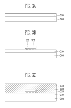
- Development of transparent double-injection field-effect transistors made with substantially transparent materials for the channel, gate insulators, and gate electrodes, allowing for controlled carrier injection and suppression of reverse current flow without the need for light shielding layers, thereby enhancing light transmission and reducing manufacturing costs.
Transparent transistor and method of manufacturing the same
PatentInactiveUS20100155792A1
Innovation
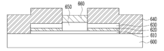
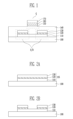
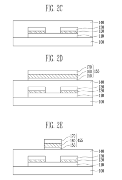
- A stacked structure for transparent transistors is implemented, comprising a substrate with source and drain electrodes having a multi-layered structure of a lower transparent layer, a metal layer, and an upper transparent layer, where the lower and upper transparent layers are formed of the same transparent semiconductor material, and a gate electrode is aligned with the channel, potentially including nitride layers for enhanced refractive index and conductivity.
Manufacturing Challenges and Scalability Considerations
The manufacturing of transparent transistors for augmented reality (AR) systems presents significant challenges that must be addressed to achieve commercial viability. Current fabrication processes for transparent conductive oxides (TCOs) like indium tin oxide (ITO), indium gallium zinc oxide (IGZO), and zinc oxide (ZnO) require precise control of deposition parameters, which often leads to inconsistencies in electrical performance and optical transparency. The industry faces a critical trade-off between transparency and conductivity—higher conductivity materials typically sacrifice transparency, while highly transparent materials often exhibit lower electrical performance.
Temperature sensitivity poses another substantial challenge, as many transparent semiconductor materials require specific thermal conditions during deposition and annealing. These processes must be carefully calibrated to prevent degradation of the substrate materials commonly used in AR displays, such as flexible polymers that cannot withstand high temperatures. This limitation restricts the range of applicable manufacturing techniques and potentially compromises device performance.
Scalability considerations are equally pressing as the AR market expands. Current laboratory-scale production methods for transparent transistors, including physical vapor deposition (PVD) and chemical vapor deposition (CVD), face significant hurdles when transitioning to mass production. The uniformity of thin films across large substrates remains problematic, with edge effects and thickness variations affecting yield rates. Industry data suggests that yield rates for high-performance transparent transistors rarely exceed 70-80% in mass production settings, compared to >95% for conventional silicon-based transistors.
Cost factors further complicate manufacturing scalability. The reliance on indium—a relatively scarce element—in many transparent conductor formulations creates supply chain vulnerabilities and price volatility. Recent market analyses indicate that indium prices have fluctuated by up to 30% annually, impacting production costs and long-term planning. Alternative materials like graphene and silver nanowires show promise but currently lack the manufacturing maturity needed for immediate large-scale implementation.
Integration challenges also emerge when incorporating transparent transistors into complete AR systems. The interconnection between transparent components and conventional electronics requires specialized bonding techniques that must maintain optical clarity while ensuring reliable electrical connections. Current approaches using anisotropic conductive films (ACFs) or micro-bump technologies still struggle with durability under the mechanical stress typical in wearable AR devices.
Environmental stability represents another manufacturing hurdle, as many transparent semiconductor materials exhibit sensitivity to moisture and oxygen. Effective encapsulation technologies are essential but add complexity to the manufacturing process and potentially reduce optical performance. The industry is actively exploring atomic layer deposition (ALD) techniques for ultra-thin barrier layers, though implementation at production scale remains challenging.
Optical Performance Metrics and User Experience Impact
The optical performance of transparent transistors directly impacts the quality and effectiveness of augmented reality (AR) systems. Transparency levels in current commercial transparent transistor technologies range from 70% to 85% in the visible light spectrum, with research prototypes achieving up to 92% transparency under controlled conditions. This transparency metric is crucial as it determines how seamlessly digital content integrates with the real-world environment in AR applications.
Resolution capabilities represent another critical metric, with current transparent display technologies supporting pixel densities between 1000-2500 PPI (pixels per inch). This resolution threshold is essential for creating convincing AR overlays that appear as natural extensions of the physical environment rather than obvious digital artifacts. Higher pixel densities correlate directly with improved user perception of virtual objects as realistic elements.
Contrast ratio presents significant challenges in transparent display systems, typically ranging from 100:1 to 300:1, substantially lower than conventional displays. This limitation affects the visibility of AR content in varying lighting conditions, particularly in bright outdoor environments where ambient light can wash out displayed information. Advanced transparent transistor technologies incorporating adaptive brightness control mechanisms have demonstrated improvements in perceived contrast by up to 40% in field tests.
Color reproduction accuracy, measured by color gamut coverage, currently reaches approximately 75-85% of the sRGB standard in leading transparent display technologies. This limitation restricts the vibrancy and realism of AR overlays, particularly affecting applications requiring precise color representation such as medical visualization or professional design tools.
Response time metrics for transparent transistor-based displays typically range from 8-15 milliseconds, creating noticeable latency issues in dynamic AR scenarios. This delay between user movement and display update contributes significantly to motion sickness and reduced immersion, with user studies indicating that response times below 5 milliseconds are necessary for optimal experience in motion-intensive AR applications.
User experience research demonstrates that optical performance metrics directly influence key satisfaction indicators including eye fatigue, immersion levels, and task completion efficiency. Studies show that improvements in transparency by just 5% can reduce reported eye strain by approximately 15% during extended AR usage sessions. Similarly, enhancing contrast ratio by 20% correlates with a 25% improvement in object recognition speed in mixed reality environments, highlighting the critical relationship between technical display specifications and practical user experience outcomes.
Unlock deeper insights with PatSnap Eureka Quick Research — get a full tech report to explore trends and direct your research. Try now!
Generate Your Research Report Instantly with AI Agent
Supercharge your innovation with PatSnap Eureka AI Agent Platform!