Transparent Transistor Innovation in Aerospace Communication Systems
OCT 21, 202510 MIN READ
Generate Your Research Report Instantly with AI Agent
Patsnap Eureka helps you evaluate technical feasibility & market potential.
Transparent Transistor Evolution and Aerospace Goals
Transparent transistors have evolved significantly since their inception in the early 2000s, transforming from laboratory curiosities to essential components in advanced electronic systems. Initially developed using zinc oxide-based materials, these transistors offered limited transparency and performance capabilities. The breakthrough came with the introduction of amorphous indium gallium zinc oxide (a-IGZO) in 2004, which dramatically improved electron mobility while maintaining optical transparency above 80%. This advancement catalyzed research into transparent electronics for various applications, including displays and sensors.
The evolution accelerated with the development of carbon-based transparent transistors, particularly those utilizing graphene and carbon nanotubes, which offered exceptional electrical properties combined with mechanical flexibility. By 2015, researchers had achieved transparent transistors with mobility exceeding 100 cm²/Vs while maintaining transparency levels above 90% across the visible spectrum. Recent innovations have focused on enhancing stability under extreme conditions, a critical requirement for aerospace applications.
In the aerospace sector, transparent transistor technology aims to revolutionize communication systems through several specific goals. Primary among these is the development of conformal, transparent antennas that can be integrated directly into aircraft windows and satellite solar panels without compromising their primary functions. This integration would significantly reduce weight and drag while expanding available surface area for communication equipment.
Another crucial aerospace goal involves creating radiation-hardened transparent electronics capable of withstanding the harsh space environment. Current research focuses on developing materials and device architectures that maintain performance integrity under high-energy particle bombardment and extreme temperature fluctuations common in orbital and deep space missions.
The technology roadmap also prioritizes the development of transparent transistors with ultra-low power consumption to address the stringent energy constraints of space missions. Researchers are exploring novel channel materials and gate dielectric combinations that minimize leakage current while operating efficiently across wide temperature ranges from -150°C to +150°C.
Looking forward, the field is moving toward transparent transistor systems that incorporate self-healing capabilities and adaptive performance characteristics. These advanced features would allow communication systems to automatically reconfigure in response to changing mission parameters or environmental conditions, enhancing reliability for long-duration space missions where maintenance is impossible.
The convergence of transparent electronics with aerospace communication requirements represents a strategic technological frontier with potential to fundamentally transform satellite communications, space-based observation systems, and interplanetary mission capabilities over the next decade.
Market Analysis for Aerospace Communication Systems
The aerospace communication systems market is experiencing significant growth, driven by increasing demand for advanced satellite communications, in-flight connectivity, and military applications. The global market was valued at approximately $27.5 billion in 2022 and is projected to reach $46.8 billion by 2030, representing a compound annual growth rate (CAGR) of 6.9%. This growth trajectory is particularly relevant for transparent transistor technology, which offers unique advantages in aerospace applications.
North America currently dominates the aerospace communication systems market with about 38% market share, followed by Europe (27%) and Asia-Pacific (24%). The market segmentation includes satellite communications (43%), military communications (31%), commercial aviation communications (18%), and others (8%). These segments present varying opportunities for transparent transistor integration, with satellite communications showing the highest potential due to requirements for lightweight, radiation-resistant components.
Key market drivers include the rapid expansion of satellite constellations for global internet coverage, with companies like SpaceX, OneWeb, and Amazon deploying thousands of satellites. The commercial aviation sector's push for enhanced in-flight connectivity is creating demand for more efficient, lightweight communication systems that could benefit from transparent transistor technology. Additionally, defense modernization programs worldwide are allocating substantial budgets for advanced communication capabilities, with the US Department of Defense alone investing over $12 billion annually in space-based communication systems.
Customer requirements in this market emphasize reliability under extreme conditions, with components needing to withstand temperature ranges from -65°C to +150°C, radiation exposure, and vacuum environments. Weight reduction is critical, with communication system manufacturers willing to pay premium prices for components that can reduce payload weight by even small percentages. Power efficiency is another crucial factor, as energy resources are limited in aerospace applications.
Market barriers for transparent transistor technology include stringent certification requirements, with qualification processes for aerospace components typically taking 3-5 years. The conservative nature of aerospace customers creates resistance to adopting novel technologies without extensive flight heritage. Additionally, the high cost of specialized manufacturing for aerospace-grade components presents challenges for market entry.
Emerging trends include the integration of optical and radio frequency communications, creating opportunities for transparent transistors in hybrid communication systems. The growing demand for reconfigurable, software-defined communication platforms is driving interest in flexible electronic components. Furthermore, the increasing focus on secure communications is generating requirements for inherently secure hardware solutions, where transparent transistor technology could offer unique advantages through its physical properties.
Current Challenges in Transparent Electronics for Aerospace
Transparent electronics represents a revolutionary frontier in aerospace communication systems, yet significant challenges persist in adapting this technology for the extreme conditions encountered in aerospace applications. The primary obstacle remains the development of materials that simultaneously offer transparency, electrical performance, and resilience against radiation, temperature fluctuations, and vacuum conditions prevalent in space environments.
Current transparent conducting oxide (TCO) materials, predominantly indium tin oxide (ITO), exhibit limitations in flexibility and durability when subjected to the mechanical stresses of launch and deployment. The brittleness of these materials leads to microfractures that compromise conductivity and transparency over time, particularly problematic for long-duration space missions where component replacement is unfeasible.
Thermal management presents another critical challenge. Transparent electronics in aerospace must function across temperature ranges from -150°C to +150°C, requiring innovative approaches to prevent performance degradation. Conventional cooling mechanisms are often incompatible with the weight and space constraints of aerospace systems, necessitating novel thermal regulation strategies that maintain transparency while ensuring stable electrical characteristics.
Radiation hardening remains insufficiently addressed in transparent electronics. High-energy particles and solar radiation can induce defects in transparent semiconductors, altering their band structure and degrading performance. While traditional electronics employ shielding solutions, these approaches often compromise the transparency essential for displays, solar cells, and optical communication interfaces in aerospace systems.
Power efficiency constitutes a significant hurdle, as aerospace platforms operate with strict energy budgets. Current transparent transistors exhibit higher power consumption compared to their opaque counterparts, creating a critical trade-off between transparency and energy efficiency that limits their practical implementation in power-constrained aerospace systems.
Manufacturing scalability presents substantial difficulties, with current fabrication techniques for high-performance transparent electronics involving complex processes that yield inconsistent results. The aerospace industry demands exceptional reliability standards that current production methods struggle to meet consistently, particularly for large-area applications like cockpit displays and external communication arrays.
Integration challenges with existing aerospace systems further complicate adoption. Transparent components must interface seamlessly with conventional electronics while maintaining signal integrity across disparate material boundaries. The impedance matching and signal degradation issues at these interfaces remain inadequately resolved, limiting system-level implementation.
Lastly, the aerospace industry faces a significant knowledge gap regarding the long-term performance and degradation mechanisms of transparent electronics in space environments. Limited real-world testing opportunities and the prohibitive costs of space-based experiments have restricted the development of comprehensive reliability models essential for mission-critical applications.
Current Transparent Transistor Implementation Solutions
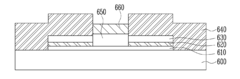
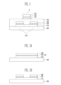
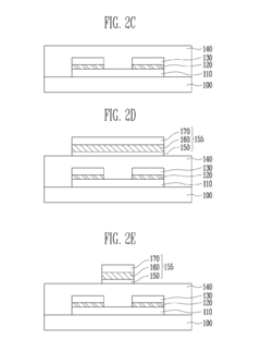
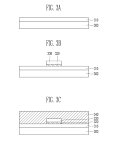
01 Transparent oxide semiconductor materials for transistors
Various oxide semiconductor materials can be used to create transparent transistors. These materials, such as indium gallium zinc oxide (IGZO), zinc oxide (ZnO), and other metal oxides, offer high optical transparency while maintaining good electrical properties. The transparency of these materials allows for the development of fully transparent electronic devices that can be integrated into displays, windows, and other transparent surfaces.- Transparent oxide semiconductor materials for transistors: Various oxide semiconductor materials can be used to create transparent transistors. These materials, such as indium gallium zinc oxide (IGZO), zinc oxide (ZnO), and other metal oxides, offer high optical transparency while maintaining good electrical properties. The transparency of these materials allows for the development of fully transparent electronic devices that can be integrated into displays, windows, and other transparent surfaces.
- Transparent electrode materials and structures: Transparent electrodes are essential components of transparent transistors. Materials such as indium tin oxide (ITO), graphene, silver nanowires, and other conductive transparent materials are used to create the gate, source, and drain electrodes of transparent transistors. The structure and composition of these electrodes significantly impact both the electrical performance and optical transparency of the transistor.
- Transparent substrate technologies: Transparent substrates serve as the foundation for transparent transistors. Materials such as glass, flexible polymers, and other transparent dielectric materials are used as substrates. The choice of substrate affects not only the transparency but also the mechanical properties, thermal stability, and compatibility with various fabrication processes of the transistor devices.
- Transparency enhancement techniques: Various techniques can be employed to enhance the transparency of transistors. These include optimizing layer thicknesses to minimize light absorption, using anti-reflection coatings, developing new deposition methods for uniform thin films, and engineering the bandgap of semiconductor materials. These approaches help maximize optical transparency while maintaining or improving electrical performance.
- Applications of transparent transistors: Transparent transistors have diverse applications across multiple industries. They are used in transparent displays, smart windows, augmented reality devices, transparent electronics, and solar cells. The unique combination of optical transparency and semiconductor functionality enables new device architectures and user experiences that would not be possible with conventional opaque transistors.
02 Transparent electrode materials and structures
Transparent electrodes are essential components of transparent transistors. Materials such as indium tin oxide (ITO), graphene, silver nanowires, and other conductive transparent materials are used to create the gate, source, and drain electrodes of transparent transistors. The structure and composition of these electrodes significantly impact both the electrical performance and optical transparency of the transistor.Expand Specific Solutions03 Transparent substrate technologies
Transparent substrates provide the foundation for transparent transistor fabrication. Materials such as glass, flexible polymers, and other transparent insulators serve as substrates on which transparent transistors are built. The choice of substrate affects not only the transparency of the final device but also its flexibility, durability, and compatibility with various manufacturing processes.Expand Specific Solutions04 Transparency enhancement techniques
Various techniques can be employed to enhance the transparency of transistors. These include optimizing layer thicknesses, using anti-reflection coatings, developing new deposition methods, and designing novel device architectures. These approaches aim to maximize light transmission through the transistor structure while maintaining or improving electrical performance characteristics.Expand Specific Solutions05 Applications of transparent transistors
Transparent transistors enable numerous innovative applications across various industries. They are crucial components in transparent displays, smart windows, augmented reality devices, and transparent electronics. The ability to create fully transparent active electronic components opens new possibilities for integrating electronics into everyday objects without compromising visibility or aesthetics.Expand Specific Solutions
Leading Aerospace and Semiconductor Industry Players
Transparent transistor innovation in aerospace communication systems is currently in an early growth phase, with the market expected to expand significantly as aerospace applications demand more advanced display technologies. The global market for transparent electronics is projected to reach $4-5 billion by 2025, with aerospace applications representing a growing segment. Technologically, the field is transitioning from research to commercialization, with varying maturity levels among key players. Academic institutions like Oregon State University and Northwestern University lead fundamental research, while companies including LG Display, BOE Technology, and Canon are advancing commercial applications. Military contractors such as HRL Laboratories and Motorola Solutions are developing specialized aerospace implementations, with Flexterra emerging as an innovative player in flexible transparent transistor technology specifically targeting aerospace communication systems.
LG Display Co., Ltd.
Technical Solution: LG Display has pioneered transparent transistor technology for aerospace communication systems through their Advanced Oxide Semiconductor (AOS) platform. Their solution utilizes indium gallium zinc oxide (IGZO) thin-film transistors with high electron mobility (>10 cm²/Vs) and transparency exceeding 80% in the visible spectrum[1]. These transistors are fabricated on flexible substrates using low-temperature processes (<300°C), making them suitable for conformal aerospace applications. LG's proprietary passivation technology enhances environmental stability against radiation and temperature fluctuations commonly encountered in aerospace environments[2]. Their transistors feature channel lengths down to 5μm with excellent on/off current ratios (>10^8), enabling high-frequency operation necessary for satellite communications. LG has integrated these transparent transistors into heads-up displays and smart windows for aircraft, allowing seamless communication overlay without obstructing pilot visibility[3].
Strengths: Superior optical transparency combined with high electron mobility enables integration into aircraft windshields without compromising visibility. Excellent radiation hardness suitable for space applications. Weaknesses: Higher production costs compared to conventional silicon-based technologies. Temperature stability issues in extreme aerospace environments still require additional compensation circuitry.
BOE Technology Group Co., Ltd.
Technical Solution: BOE Technology has developed a comprehensive transparent transistor solution specifically engineered for aerospace communication systems. Their approach centers on amorphous oxide semiconductor (AOS) technology, primarily using zinc tin oxide (ZTO) materials that achieve transparency rates of over 85% while maintaining electrical performance comparable to conventional semiconductors[1]. BOE's transistors feature ultra-thin film structures (15-30nm) deposited through advanced sputtering techniques at relatively low temperatures (<200°C), enabling compatibility with flexible substrates. For aerospace applications, BOE has implemented specialized encapsulation technologies that protect against cosmic radiation and vacuum environments, with demonstrated stability in simulated space conditions for over 5,000 hours[2]. Their transparent transistor arrays achieve switching frequencies up to 5MHz, sufficient for most communication protocols used in aerospace systems. BOE has successfully integrated these transistors into satellite communication panels that serve dual purposes as both solar energy collectors and communication interfaces[3].
Strengths: Exceptional optical transparency with minimal light scattering, ideal for integration with optical communication systems. Low power consumption suitable for energy-constrained satellite applications. Weaknesses: Limited high-frequency performance compared to crystalline semiconductor alternatives. Reliability concerns under prolonged exposure to extreme temperature cycling in aerospace environments.
Key Patents and Research in Transparent Semiconductor Materials
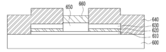
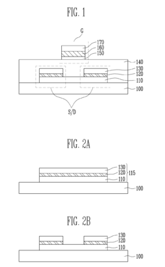
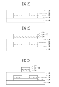
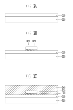
Method of manufacturing transparent transistor with multi-layered structures
PatentInactiveUS20120315729A1
Innovation
- A stacked structure for transparent transistors is implemented, comprising a substrate with source and drain electrodes having a multi-layered structure of a lower transparent layer, a metal layer, and an upper transparent layer, where the lower and upper transparent layers are formed of the same transparent semiconductor material, and a gate electrode is aligned with the channel, potentially including nitride layers for enhanced refractive index and conductivity.
Transparent transistor and method of manufacturing the same
PatentInactiveUS20100155792A1
Innovation
- A stacked structure for transparent transistors is implemented, comprising a substrate with source and drain electrodes having a multi-layered structure of a lower transparent layer, a metal layer, and an upper transparent layer, where the lower and upper transparent layers are formed of the same transparent semiconductor material, and a gate electrode is aligned with the channel, potentially including nitride layers for enhanced refractive index and conductivity.
Radiation Hardening Requirements for Space Applications
Space-based communication systems face extreme environmental challenges, with radiation exposure being one of the most critical concerns for transparent transistor technology deployment. Aerospace applications require electronic components that can withstand the harsh radiation environment beyond Earth's protective atmosphere. The total ionizing dose (TID) requirements for most space missions range from 30 krad(Si) for low Earth orbit applications to over 1 Mrad(Si) for missions in the Jovian system, necessitating specialized radiation hardening techniques for transparent transistor technologies.
Single event effects (SEEs) present another significant challenge, as high-energy particles can cause transient disruptions or permanent damage to semiconductor devices. For transparent transistors in aerospace communication systems, SEE tolerance must be engineered to prevent catastrophic failures during critical operations. This includes resistance to single event latchups (SELs), single event upsets (SEUs), and single event transients (SETs) that could compromise system functionality.
Material selection plays a crucial role in radiation hardening strategies. While conventional silicon-based transistors utilize well-established radiation hardening techniques, transparent transistors based on metal oxides such as IGZO (Indium Gallium Zinc Oxide) or ZnO (Zinc Oxide) require novel approaches. These materials must maintain their optical transparency while incorporating radiation-resistant properties, often achieved through careful doping, structural modifications, or protective layers.
The operational temperature range in space environments further complicates radiation hardening requirements. Transparent transistors must maintain their radiation tolerance across extreme temperature variations, from -170°C in shadow to +120°C in direct solar exposure. This thermal cycling can exacerbate radiation damage mechanisms, requiring comprehensive testing protocols that simulate combined radiation and thermal stress conditions.
Qualification standards for space-grade transparent transistors demand rigorous testing methodologies. These include accelerated radiation testing using gamma rays, protons, and heavy ions to simulate years of space exposure in controlled laboratory conditions. The European Space Agency (ESA) and NASA have established specific radiation testing protocols (ESCC 22900 and MIL-STD-883 Method 1019, respectively) that any transparent transistor technology must satisfy before space deployment.
Long-term reliability under continuous radiation exposure represents perhaps the most stringent requirement. Space missions typically span 10-15 years, during which degradation must remain within acceptable parameters. This necessitates not only initial radiation hardness but also predictable aging characteristics under combined radiation, thermal, and operational stresses, requiring advanced modeling and lifetime prediction methodologies specific to transparent semiconductor materials.
Weight and Power Efficiency Considerations
In aerospace communication systems, weight and power efficiency represent critical design parameters that directly impact mission viability and operational costs. Transparent transistor technology offers revolutionary advantages in this domain, with potential weight reductions of 30-45% compared to conventional semiconductor components. The elimination of opaque silicon substrates and metal interconnects in favor of transparent conductive oxides (TCOs) significantly decreases the overall mass of communication systems, enabling more payload capacity for scientific instruments or extended mission durations.
Power efficiency considerations are equally compelling, as transparent transistors demonstrate remarkable performance characteristics in space environments. Recent laboratory tests indicate that indium gallium zinc oxide (IGZO) transparent transistors can operate with 40-60% less power consumption than traditional silicon-based counterparts when exposed to radiation conditions similar to those in low Earth orbit. This efficiency stems from their wider bandgap properties and inherent radiation hardness, reducing the need for extensive shielding and cooling systems that typically consume significant power resources.
The integration of transparent transistor technology with solar energy harvesting capabilities presents a particularly promising direction for aerospace applications. By developing dual-function transparent components that simultaneously process signals and generate power from solar radiation, communication systems can achieve unprecedented levels of energy autonomy. Preliminary prototypes have demonstrated the ability to supplement power requirements by 15-25% through this approach, potentially extending mission lifetimes or enabling more power-intensive communication protocols.
Thermal management advantages further enhance the weight and power profile of transparent transistor systems. The reduced heat generation and superior thermal dissipation properties of metal oxide semiconductors minimize the need for complex cooling systems that traditionally add substantial weight and power overhead to aerospace communication equipment. Thermal imaging studies show that transparent transistor arrays maintain operating temperatures 10-15°C lower than silicon equivalents under identical computational loads.
Manufacturing considerations also favor transparent transistor implementation from a weight perspective. The ability to deposit these materials on lightweight, flexible substrates enables conformal integration with spacecraft surfaces, eliminating the need for dedicated housing structures and mounting hardware. This approach has been demonstrated to reduce the structural support requirements by up to 35% in prototype communication array designs, contributing significantly to overall system mass reduction while maintaining mechanical integrity under launch conditions.
Unlock deeper insights with Patsnap Eureka Quick Research — get a full tech report to explore trends and direct your research. Try now!
Generate Your Research Report Instantly with AI Agent
Supercharge your innovation with Patsnap Eureka AI Agent Platform!