

Why Transparent Transistors are Vital for Smart Infrastructure Development
OCT 21, 202510 MIN READ
Generate Your Research Report Instantly with AI Agent
PatSnap Eureka helps you evaluate technical feasibility & market potential.
Transparent Transistor Technology Evolution and Objectives
Transparent transistor technology has evolved significantly over the past three decades, transforming from laboratory curiosities to essential components in modern electronics. The journey began in the early 1990s with the first demonstrations of transparent conducting oxides (TCOs) as active semiconductor materials. These early iterations suffered from poor mobility and stability issues, limiting their practical applications. By the early 2000s, researchers achieved a breakthrough with amorphous oxide semiconductors (AOS), particularly indium gallium zinc oxide (IGZO), which offered improved electron mobility while maintaining optical transparency.
The mid-2000s marked a pivotal moment when transparent thin-film transistors (TTFTs) began transitioning from research laboratories to commercial applications, initially in display technologies. This period saw significant improvements in material composition, deposition techniques, and device architectures, leading to enhanced performance metrics including higher mobility, better stability, and increased transparency in the visible spectrum.
Recent developments have focused on expanding material options beyond traditional metal oxides to include organic semiconductors, carbon-based materials like graphene, and hybrid organic-inorganic compounds. These alternatives offer advantages such as flexibility, lower processing temperatures, and compatibility with various substrates, opening new application possibilities in smart infrastructure.
The evolution trajectory has been driven by several key objectives. Primary among these is achieving higher electron mobility while maintaining optical transparency above 80% in the visible spectrum. Another critical goal has been improving operational stability under various environmental conditions, particularly humidity and temperature fluctuations, which is essential for outdoor smart infrastructure applications.
Energy efficiency represents another fundamental objective, with research focusing on reducing operating voltages and power consumption to enable battery-powered or energy-harvesting applications in distributed sensor networks for smart cities. Concurrently, efforts have been directed toward developing fabrication methods compatible with large-area processing and low-temperature deposition to enable integration with temperature-sensitive substrates.
Looking forward, the technology aims to achieve seamless integration with other electronic components and sensing technologies to create truly invisible electronics that can be embedded in everyday objects and infrastructure. The ultimate objective is to develop transparent transistors that combine high performance with mechanical flexibility, environmental durability, and cost-effective manufacturing processes to enable ubiquitous deployment in smart windows, intelligent transportation systems, and augmented reality interfaces that form the backbone of next-generation smart infrastructure.
Market Demand Analysis for Smart Infrastructure Applications
The global market for smart infrastructure is experiencing unprecedented growth, driven by urbanization, digital transformation, and the need for sustainable development. Transparent transistors represent a critical enabling technology in this evolving landscape, with market demand accelerating across multiple application domains.
Smart cities constitute the primary market driver, with projections indicating that over 70% of the world's population will live in urban areas by 2050. This demographic shift necessitates intelligent infrastructure capable of monitoring and managing resources efficiently. Transparent transistors enable the development of smart windows, interactive displays, and invisible sensors that can be seamlessly integrated into urban environments without disrupting aesthetics or functionality.
The building automation sector demonstrates particularly strong demand, with the market for smart building technologies expanding at a compound annual growth rate of approximately 12%. Property developers and managers increasingly seek solutions that can enhance energy efficiency while maintaining architectural integrity. Transparent transistors allow for the integration of control systems directly into glass surfaces and structural elements, eliminating the need for visible hardware.
Transportation infrastructure represents another significant market opportunity. As governments worldwide invest in modernizing roads, bridges, and public transit systems, demand for embedded intelligence continues to rise. Transparent transistor technology enables the development of smart windshields, interactive transit station displays, and road-embedded sensors that can monitor traffic conditions while remaining visually unobtrusive.
Energy management applications are driving substantial market interest as well. The global push toward renewable energy and grid optimization has created demand for transparent solar cells and smart grid monitoring systems. These applications benefit from transparent transistor technology that allows for power generation and monitoring without compromising visibility or design aesthetics.
Healthcare infrastructure is emerging as a rapidly growing market segment, with hospitals and clinics seeking technologies that enhance patient care while maintaining sterile environments. Transparent displays and touch interfaces powered by transparent transistors offer significant advantages in these settings, allowing for information display and interaction without creating surfaces that harbor contaminants.
Consumer expectations are further fueling market demand, as end-users increasingly expect infrastructure to be both intelligent and visually appealing. Research indicates that adoption rates for smart technologies increase by up to 35% when the technology integrates seamlessly with existing aesthetics. Transparent transistors directly address this preference by enabling functionality without visual intrusion.
Market analysis reveals that regions with advanced urban development initiatives, particularly in East Asia, North America, and Western Europe, currently demonstrate the highest demand for transparent transistor applications in smart infrastructure. However, emerging economies are showing accelerated adoption rates as they implement technology-forward infrastructure development plans.
Current Challenges in Transparent Electronics Development
Despite significant advancements in transparent electronics over the past decade, several critical challenges continue to impede widespread implementation in smart infrastructure applications. The most pressing issue remains the trade-off between transparency and performance. While conventional silicon-based transistors offer excellent electrical properties, they are inherently opaque. Conversely, transparent conducting oxides (TCOs) like indium tin oxide (ITO) and indium gallium zinc oxide (IGZO) provide optical transparency but typically demonstrate lower carrier mobility and switching speeds compared to silicon counterparts.
Material stability presents another significant hurdle. Many transparent semiconducting materials exhibit performance degradation when exposed to environmental factors such as humidity, oxygen, and ultraviolet radiation. This vulnerability severely limits their practical deployment in outdoor smart infrastructure applications where durability and reliability are paramount requirements.
Manufacturing scalability remains problematic for transparent electronics. Current fabrication techniques often involve complex processes requiring high temperatures or vacuum conditions, making mass production costly and energy-intensive. The industry lacks standardized, cost-effective manufacturing protocols that can reliably produce transparent transistors with consistent performance characteristics across large areas.
Interface engineering between different transparent materials poses substantial technical difficulties. Creating stable, low-resistance contacts between transparent conductors, semiconductors, and dielectrics requires precise control over interface properties. Defects at these interfaces often lead to charge trapping, leakage currents, and overall performance deterioration.
Power consumption optimization represents another significant challenge. While transparent electronics are theoretically ideal for energy-harvesting applications in smart buildings, current transparent transistor technologies typically require higher operating voltages than conventional silicon devices, offsetting potential energy savings.
The limited availability of certain critical raw materials further complicates development efforts. Indium, a key component in many transparent conducting oxides, faces supply constraints and price volatility. Finding abundant, environmentally friendly alternative materials with comparable performance remains an ongoing research priority.
Lastly, integration challenges persist when incorporating transparent electronics into existing infrastructure systems. Developing standardized protocols for connecting transparent electronic components with conventional electronics, power sources, and data networks requires significant engineering efforts. The lack of unified industry standards for transparent electronic components further complicates system-level integration and interoperability.
Current Implementation Solutions for Transparent Transistors
01 Transparent oxide semiconductor materials for transistors
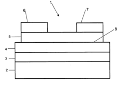
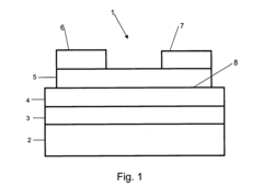
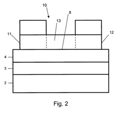
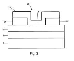
Various oxide semiconductor materials can be used to create transparent transistors. These materials, such as indium gallium zinc oxide (IGZO), zinc oxide (ZnO), and other metal oxides, offer high optical transparency while maintaining good electrical properties. The transparency of these materials allows for the development of fully transparent electronic devices that can be integrated into displays, windows, and other transparent surfaces.- Transparent oxide semiconductor materials for transistors: Various oxide semiconductor materials are used to create transparent transistors. These materials, such as zinc oxide, indium gallium zinc oxide (IGZO), and other metal oxides, offer high electron mobility while maintaining optical transparency. The unique properties of these materials allow for the fabrication of transistors that can transmit visible light while still functioning as effective electronic components, making them suitable for transparent display applications.
- Transparent display technologies incorporating transparent transistors: Transparent displays utilize transparent transistors as key components in their pixel driving circuits. These displays can show information while allowing viewers to see through them, enabling augmented reality applications and heads-up displays. The integration of transparent transistors enables the creation of display panels with varying levels of transparency that can be adjusted according to user needs, providing both information display and see-through capabilities.
- Fabrication methods for transparent transistor structures: Various fabrication techniques are employed to create transparent transistor structures. These include thin-film deposition methods such as sputtering, chemical vapor deposition, and solution processing. Special attention is given to electrode materials and configurations to maintain transparency while ensuring good electrical contact. Post-deposition treatments like annealing are used to optimize the transparency and electrical performance of the transistors.
- Transparent conductive electrodes for transistor applications: Transparent conductive materials are essential for creating the electrodes in transparent transistors. Materials such as indium tin oxide (ITO), fluorine-doped tin oxide (FTO), and conductive polymers provide the necessary electrical conductivity while maintaining optical transparency. Novel nanomaterials like graphene and silver nanowires are also being explored as alternative transparent electrode materials to improve performance and reduce costs.
- Applications of transparent transistors in electronic devices: Transparent transistors find applications in various electronic devices beyond displays, including transparent sensors, smart windows, and wearable electronics. These transistors enable the development of invisible circuits that can be integrated into everyday objects without affecting their appearance. The combination of electrical functionality and optical transparency opens up new possibilities for interactive surfaces and Internet of Things (IoT) devices that blend seamlessly with their surroundings.
02 Transparent electrode materials and structures
Transparent electrodes are essential components of transparent transistors. Materials such as indium tin oxide (ITO), graphene, silver nanowires, and other conductive transparent materials are used to create the gate, source, and drain electrodes of transparent transistors. The structure and composition of these electrodes significantly impact the overall transparency and performance of the transistor devices.Expand Specific Solutions03 Fabrication techniques for transparent transistors
Various fabrication methods are employed to create transparent transistors with high transparency and performance. These include low-temperature deposition processes, solution processing, photolithography, and other techniques that enable the creation of uniform transparent films and precise patterning. Advanced fabrication techniques help to minimize defects and optimize the transparency and electrical characteristics of the transistors.Expand Specific Solutions04 Integration of transparent transistors in display technologies
Transparent transistors are increasingly being integrated into various display technologies, including LCDs, OLEDs, and transparent displays. The high transparency of these transistors allows for improved light transmission through the display, resulting in brighter, more energy-efficient displays. Additionally, transparent transistors enable the development of novel display applications such as heads-up displays, augmented reality devices, and transparent screens.Expand Specific Solutions05 Performance optimization for transparent transistor applications
Various methods are employed to optimize the performance of transparent transistors while maintaining high transparency. These include doping strategies, interface engineering, multilayer structures, and annealing treatments. These optimization techniques aim to balance the trade-off between transparency and electrical performance, addressing challenges such as carrier mobility, stability, and uniformity across large areas.Expand Specific Solutions
Leading Companies and Research Institutions in Transparent Electronics
The transparent transistor market is in a growth phase, characterized by increasing adoption in smart infrastructure applications. With an estimated market size of $3-5 billion and projected annual growth of 15-20%, this technology is transitioning from research to commercial applications. Technical maturity varies across players: academic institutions (Oregon State University, Northwestern University, Peking University) lead fundamental research; established electronics giants (Intel, Samsung Display, LG Display, BOE Technology) focus on manufacturing scalability; while specialized firms (Semiconductor Energy Laboratory, TCL China Star) develop niche applications. The ecosystem shows regional concentration in East Asia, with collaborative R&D between universities and industry accelerating development of high-performance, cost-effective transparent transistors essential for next-generation smart infrastructure.
Oregon State University
Technical Solution: Oregon State University has pioneered fundamental research in transparent transistor technology that has shaped the entire field. Their groundbreaking work with amorphous oxide semiconductors, particularly zinc tin oxide (ZTO) and indium gallium zinc oxide (IGZO), has established the scientific foundation for transparent electronics in smart infrastructure. OSU researchers have developed novel solution-processing techniques that enable low-cost fabrication of transparent transistors on various substrates including glass, plastic, and even paper. Their approach utilizes environmentally friendly precursors and low-temperature processing (<300°C), making it compatible with temperature-sensitive materials used in infrastructure. The university has demonstrated transparent transistor arrays with field-effect mobility exceeding 10 cm²/Vs while maintaining optical transparency above 80% across the visible spectrum. Their technology has been applied to prototype smart windows that dynamically control light transmission based on environmental conditions, energy-harvesting transparent surfaces for buildings, and transparent sensor networks for infrastructure monitoring.
Strengths: Pioneering research with fundamental patents in the field; innovative low-cost fabrication approaches; strong collaboration network with industry partners. Weaknesses: Limited commercial-scale manufacturing capabilities; technology transfer dependencies; requires industry partnerships for large-scale implementation.
BOE Technology Group Co., Ltd.
Technical Solution: BOE has developed advanced oxide semiconductor-based transparent transistor technologies specifically designed for smart infrastructure applications. Their solution utilizes indium gallium zinc oxide (IGZO) transparent thin-film transistors with high electron mobility (>10 cm²/Vs) and optical transparency exceeding 80% in the visible spectrum. BOE's transparent transistors are integrated into their smart glass and transparent display systems that serve as interactive interfaces for smart buildings, transportation hubs, and urban infrastructure. The company has implemented a unique low-temperature fabrication process that allows these transistors to be manufactured on flexible substrates, enabling curved and bendable smart surfaces that can be seamlessly integrated into architectural elements. Their technology also features self-powered capabilities through integration with transparent solar cells, creating energy-autonomous smart windows and surfaces for sustainable infrastructure development.
Strengths: Industry-leading production capacity for large-area transparent displays; vertical integration from transistor fabrication to complete smart surface solutions; established supply chain for commercial deployment. Weaknesses: Higher manufacturing costs compared to conventional opaque electronics; limited performance in extreme temperature environments; requires specialized installation and maintenance.
Key Patents and Innovations in Transparent Semiconductor Materials
Transparent conductor materials with enhanced near infrared properties and methods of forming thereof
PatentActiveUS11891687B2
Innovation
- A method involving the deposition of a transparent conductive material layer, typically indium tin oxide, on a substrate followed by high-temperature annealing at least 450°C for 2 minutes, achieving a transmission of at least 70% at 1550 nm and a Haacke figure of merit of at least 40×10−4Ω−1, while maintaining low resistivity.
Transistor structures and methods for making the same
PatentInactiveUS20070141784A1
Innovation
- Development of enhancement-mode, field-effect transistors with a substantially transparent channel layer made from materials like ZnO or SnO2, which are produced by annealing, and a gate insulator layer, allowing for a transparent transistor structure that enables high optical transmission across the visible and infrared spectrum.
Integration Frameworks for Smart Infrastructure Systems
The integration of transparent transistors into smart infrastructure systems requires comprehensive frameworks that address both technical and operational challenges. These frameworks must facilitate seamless communication between various transparent electronic components while ensuring system reliability, scalability, and security. Current integration approaches typically employ layered architectures that separate hardware interfaces, data processing, and application services.
Middleware solutions have emerged as critical components in these integration frameworks, serving as intermediaries between transparent transistor-based sensors and higher-level applications. These solutions handle protocol translation, data normalization, and event processing, enabling heterogeneous transparent electronic systems to function cohesively within smart infrastructure environments.
Open standards and protocols play a fundamental role in successful integration frameworks. Standards such as OneM2M, MQTT, and CoAP provide common communication languages for transparent electronic devices, while industry-specific protocols address unique requirements in sectors like transportation, energy management, and public safety. The adoption of these standards significantly reduces integration complexity and promotes interoperability.
Edge computing architectures have become increasingly important in transparent transistor integration frameworks, allowing for distributed processing capabilities that reduce latency and bandwidth requirements. By processing data closer to transparent sensors and displays, edge computing enables real-time decision-making capabilities essential for critical infrastructure applications like traffic management and emergency response systems.
Cloud-based integration platforms complement edge computing by providing centralized data repositories, advanced analytics, and machine learning capabilities. These platforms aggregate data from distributed transparent electronic systems, enabling comprehensive analysis and visualization of infrastructure performance metrics. The hybrid edge-cloud approach optimizes both responsiveness and analytical depth.
Security frameworks represent another crucial dimension of integration, implementing multi-layered protection strategies that safeguard transparent electronic components from cyber threats. These include hardware-level security features embedded within transparent transistors, secure communication protocols, and comprehensive identity and access management systems tailored to smart infrastructure requirements.
Digital twin technologies are increasingly incorporated into integration frameworks, creating virtual replicas of physical infrastructure systems that incorporate transparent electronic components. These digital twins enable simulation, testing, and optimization of integrated systems before deployment, significantly reducing implementation risks and accelerating innovation cycles in smart infrastructure development.
Sustainability and Energy Efficiency Considerations
Transparent transistors represent a significant advancement in sustainable infrastructure development, offering remarkable energy efficiency benefits compared to conventional electronic components. These devices can operate with substantially lower power consumption while maintaining high performance, which is crucial for large-scale smart infrastructure deployments where energy demands could otherwise be prohibitive.
The integration of transparent transistors into building materials enables dual functionality without additional energy requirements. For instance, smart windows incorporating these transistors can dynamically control light transmission while simultaneously serving as display interfaces or energy harvesters, eliminating the need for separate systems and reducing overall energy consumption.
From a lifecycle perspective, transparent transistors often utilize earth-abundant materials such as zinc oxide, indium gallium zinc oxide (IGZO), or organic semiconductors that require less energy-intensive extraction and processing compared to traditional silicon-based electronics. Manufacturing processes for these materials typically operate at lower temperatures, further reducing the embodied energy in the final products.
The transparency feature itself contributes to sustainability by allowing visible light to pass through, reducing the need for artificial lighting in smart buildings. When deployed in photovoltaic applications, transparent transistors enable the development of see-through solar panels that can be integrated into windows and building facades, generating clean energy while maintaining aesthetic and functional requirements of the structure.
In IoT sensor networks for smart cities, transparent transistors enable self-powered sensing nodes through their compatibility with energy harvesting technologies. These sensors can operate autonomously for extended periods without battery replacement, dramatically reducing maintenance requirements and electronic waste generation across large-scale urban deployments.
The thermal properties of many transparent semiconductor materials also contribute to energy efficiency, as they typically generate less heat during operation compared to silicon-based alternatives. This reduces cooling requirements in dense electronic systems, which represents a significant portion of energy consumption in data centers and other computing infrastructure supporting smart city operations.
Looking forward, the continued development of transparent transistors promises further sustainability improvements through biodegradable and recyclable electronic components. Research into organic and hybrid transparent semiconductors is advancing toward fully sustainable electronic systems that minimize environmental impact throughout their lifecycle while enabling the intelligent infrastructure necessary for future smart cities and transportation networks.
Unlock deeper insights with PatSnap Eureka Quick Research — get a full tech report to explore trends and direct your research. Try now!
Generate Your Research Report Instantly with AI Agent
Supercharge your innovation with PatSnap Eureka AI Agent Platform!