Grounded gate and isolation techniques for reducing dark current in CMOS image sensors

An image sensor and sensor technology, applied in the direction of circuits, diodes, electrical components, etc., can solve problems such as high leakage current

CN1735969AInactive Publication Date: 2006-02-15APTINA IMAGING CORP
2 Cites 21 Cited by

Patent Information

Authority / Receiving Office
CN · China
Current Assignee / Owner
Publication Date
2006-02-15
Estimated Expiration
Not applicable · inactive patent

Smart Images

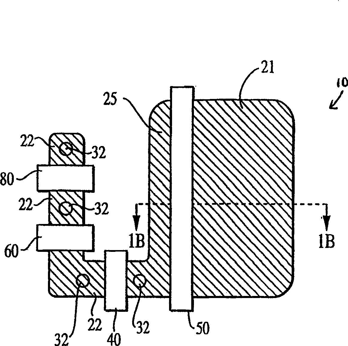
  • Figure 1
    Figure 1
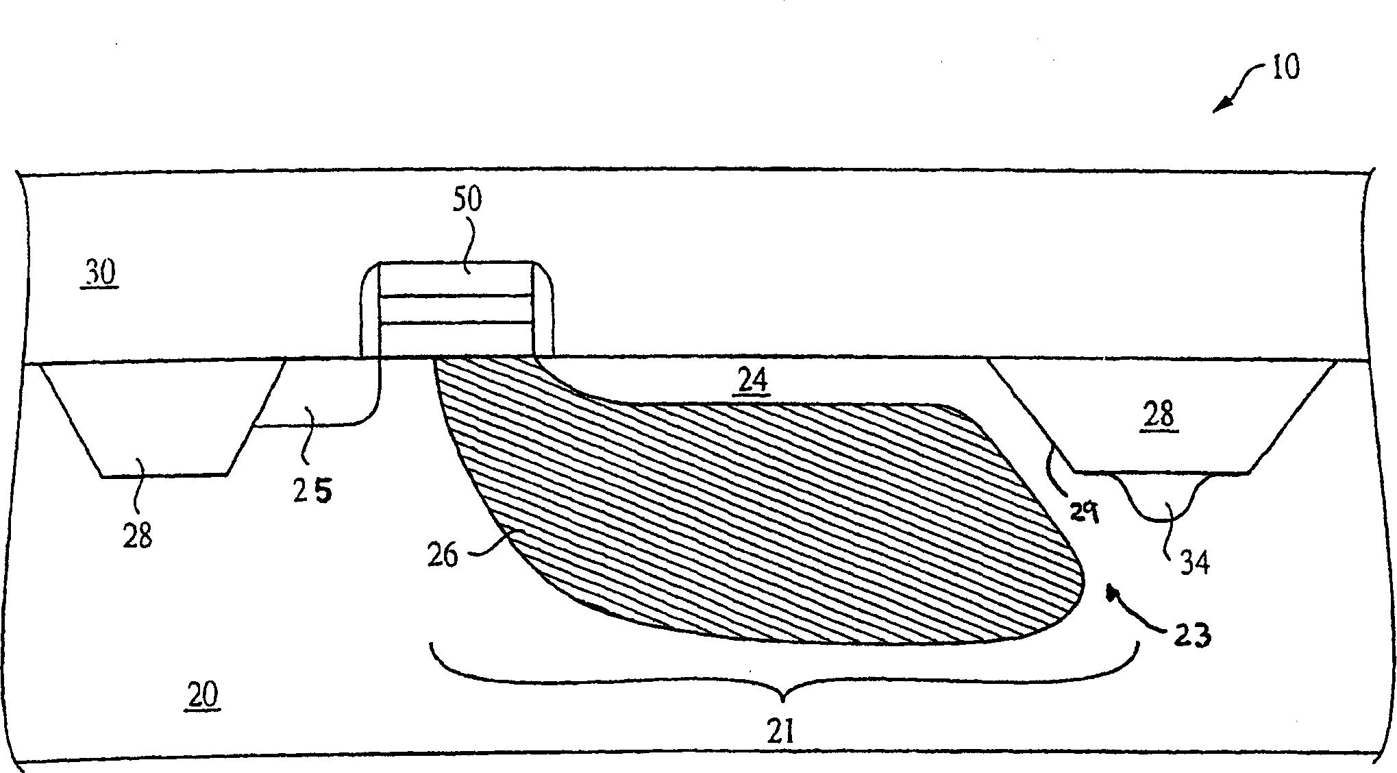
  • Figure 2
    Figure 2
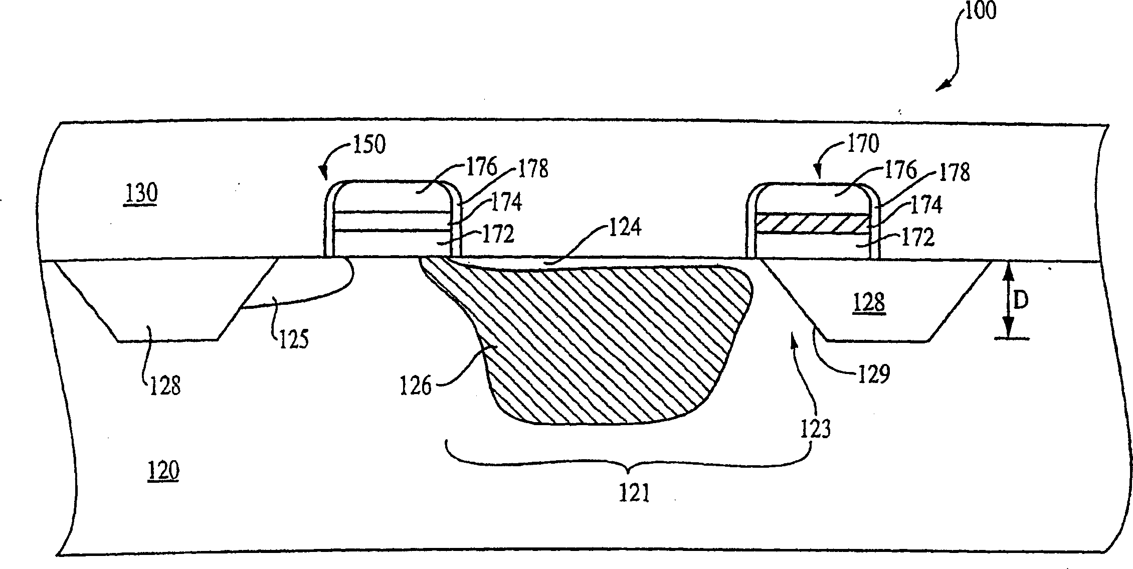
  • Figure 3
    Figure 3
Patent Text Reader

Abstract

Isolation methods and devices for isolating regions of a semiconductor device. The isolation structure and methods include forming a biased gate over a field isolation region and adjacent a pixel of an image sensor. The isolation methods also include forming an isolation gate over substantial portions of a field isolation region to isolate pixels in an array of pixels. The isolation method and structure further include forming an isolating trench in an active area and filling the trench with a doped conductive material containing silicon. There is also provided a method and structure for isolating the regions by providing a trench in an active area of a substrate, growing an epitaxial layer in the trench to fill the trench or to partially fill the trench and depositing an insulating material over the epitaxial layer and within the trench to completely fill the trench.
Need to check novelty before this filing date? Find Prior Art

Description

technical field

[0001] The present invention generally relates to a semiconductor device, and more particularly to a trench isolation technique used in a semiconductor device including a CMOS image sensor. Background technique

[0002] In silicon integrated circuit (IC) fabrication, it is often necessary to isolate semiconductor devices formed in a substrate. The same is true for many semiconductor memory devices such as DRAM, flash memory, SRAM, microprocessors, DSPs and ASICs. The individual pixels of a CMOS image sensor must also be isolated from each other.

[0003] CMOS image sensor circuitry includes a focal plane array of pixel cells, each cell including a photogate, photoconductor, or photodiode over a charge accumulation region within a substrate for accumulating photogenerated charge. Each pixel cell may include a transistor for transferring charge from the charge accumulation region to a floating diffusion node, and a transistor for resetting the diffusion node ...

Examples

Embodiment Construction

[0035] In the following detailed description, reference is made to the accompanying drawings, which form a part hereof and which represent particular embodiments in which the invention may be practiced. These embodiments have been described in sufficient detail to enable those skilled in the art to practice the invention, and it should be understood that other embodiments may be utilized and structural, Logical and electrical changes.

[0036] The terms "wafer" and "substrate" shall be understood to include silicon, silicon-on-insulator (SOI), or silicon-on-sapphire (SOS) technologies, doped and undoped semiconductors, silicon epitaxial layers supported by a base semiconductor pedestal, and other semiconductor structures. Furthermore, when referring to a "wafer" or "substrate" in the following description, previous process steps may be utilized to form regions or junctions in the base semiconductor structure or pedestal. Furthermore, the semiconductor does not have to be sil...