
Method for erasing non-volatile memory
a non-volatile memory and erasing technology, applied in static storage, digital storage, instruments, etc., can solve the problems of affecting the reliability of the device, the current leakage phenomenon of the device cannot be easily detected, and the sensitivity to the defect of the tunneling oxide layer is small, so as to reduce the time spent in erasing operations
- Summary
- Abstract
- Description
- Claims
- Application Information
AI Technical Summary
Benefits of technology
Problems solved by technology
Method used
Image

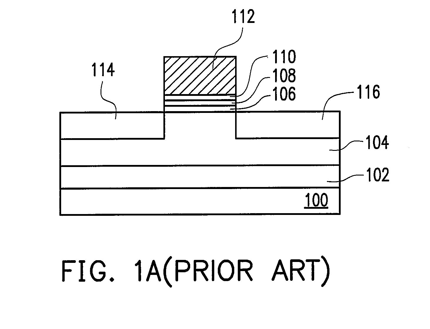
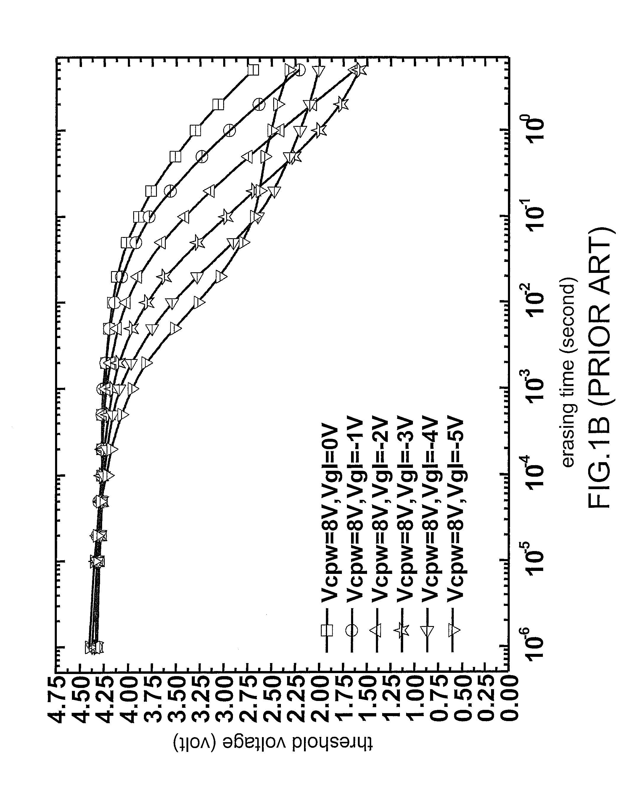
Examples
first embodiment
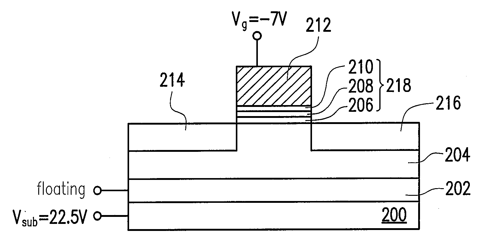
[0044]FIG. 2A is a schematic sectional view of an embodiment according to the method for erasing a non-volatile memory of the present invention. FIG. 2B is a simplified circuit diagram of FIG. 2A.
[0045]As shown in FIG. 2A, the non-volatile memory includes a first conductive type substrate 200, a second conductive type well 202, a first conductive type well 204, a bottom dielectric layer 206, a charge trapping layer 208, a top dielectric layer 210, a gate 212, a second conductive type source region 214, and a second conductive type drain region 216.
[0046]The second conductive type well 202 is, for example, disposed in the first conductive type substrate 200. The first conductive type well 204 is, for example, disposed on the second conductive type well 202. The bottom dielectric layer 206, the charge trapping layer 208, the top dielectric layer 210, and the gate 212 are, for example, disposed sequentially on the first conductive type substrate 200. The material of the bottom dielectr...
second embodiment
[0050]FIG. 3A is a schematic sectional view of another embodiment according to the method for erasing the non-volatile memory of the present invention. FIG. 3B is a simplified circuit diagram of FIG. 3A. The members in FIG. 3A that are the same as those in FIG. 2A are represented with the same labels and description thereof is omitted. Description of the differences is made herein.
[0051]As shown in FIG. 3, the second conductive type well 202 and the first conductive type well 204 constitute a Zener diode. Therefore, the second conductive type well 202 and the first conductive type well 204 have a relative high dopant concentration. For example, the dopant concentration of the conventional second conductive type well 202 and the first conductive type well 204 is generally about 5E12 / cm2. In the present invention, in order to make the second conductive type well 202 and the first conductive type well 204 constitute the Zener diode, the dopant concentration of the second conductive typ...
third embodiment
[0054]FIG. 4A is a schematic sectional view of another embodiment according to the method for erasing a non-volatile memory of the present invention. FIG. 4B is a simplified circuit diagram of FIG. 4A. The members in FIG. 4A that are the same as those in FIG. 2A are represented with the same labels and description thereof is omitted. Description of the differences is made herein.
[0055]As shown in FIG. 4B, the first conductive type substrate 200, the second conductive type well 202, and the first conductive type well 204 constitute a bipolar transistor. The gate 212, the composite dielectric layer 218, the first conductive type well 204 constitute the capacitor C.
[0056]Referring to FIG. 4A and FIG. 4B, when erasing operation is performed on the non-volatile memory, a voltage Vg is applied to the gate 212, a voltage Vsub is applied to the first conductive type substrate 200, and a voltage VDNW is applied to the second conductive type well 202. The Vsub is large enough to induce the su...
PUM
 Abstract
Description
Claims
Application Information