

Organic electroluminescence element
a technology of electroluminescence elements and organic materials, applied in the field of organic electroluminescence elements, can solve the problems of instability of elements, deterioration of luminescence efficiency, rise of drive voltage, etc., and achieve the effect of high transparency
Patent Information
- Authority / Receiving Office
- US · United States
- Patent Type
- Applications(United States)
- Current Assignee / Owner
- Publication Date
- 2010-09-23
- Estimated Expiration
- Not applicable · inactive patent
Smart Images
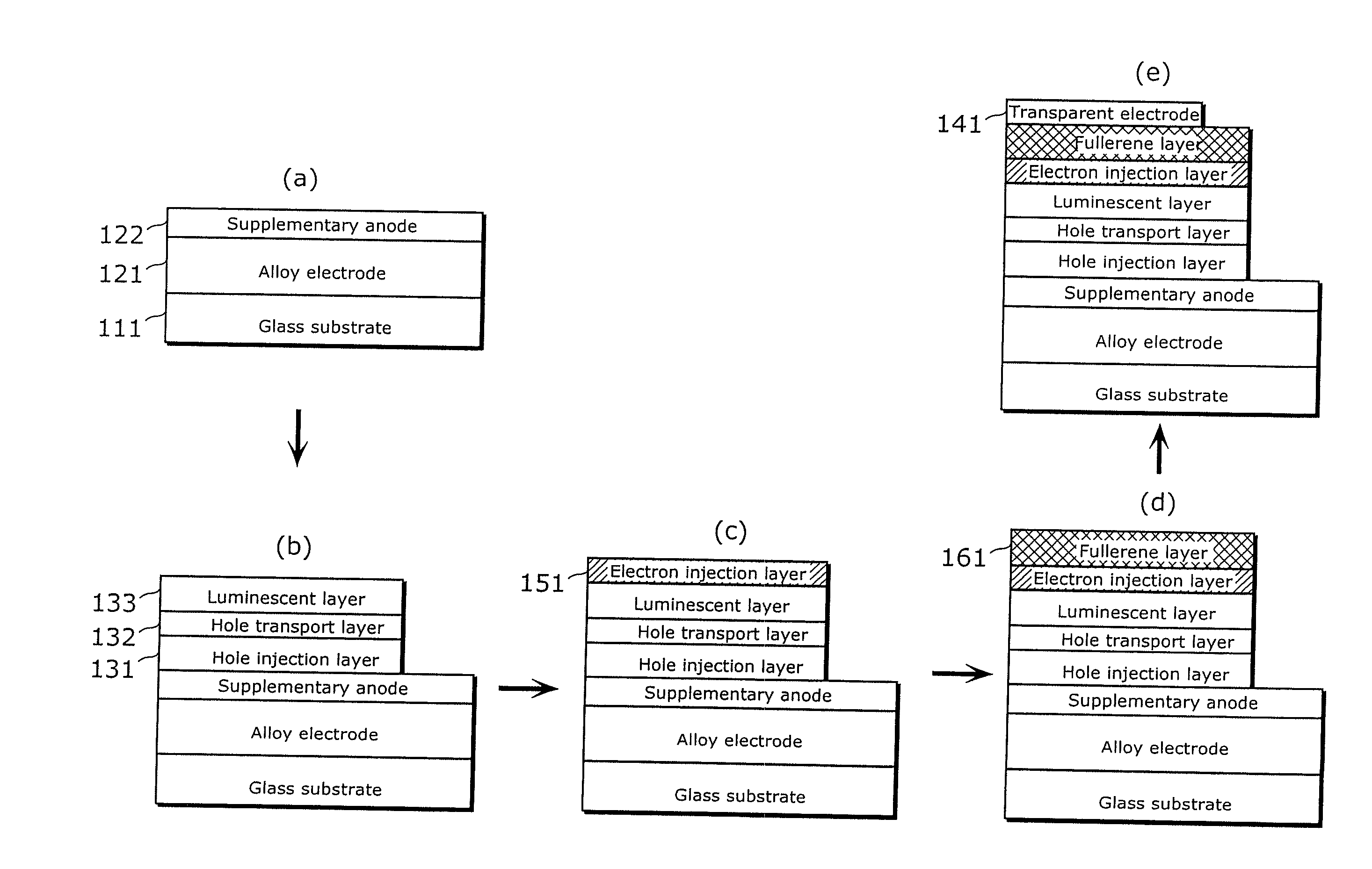
Figure 1 
Figure 2 
Figure 3
Abstract
Description
CROSS REFERENCE TO RELATED APPLICATION(S)
[0001] This is a continuation application of PCT Application No. PCT / JP2009 / 002347 filed May 27, 2009, designating the United States of America, the disclosure of which, including the specification, drawings, and claims, is incorporated herein by reference in its entirety.
[0002] The disclosure of United Kingdom Patent Application No. 0810044.8 filed on Jun. 2, 2008, including the specification, drawings and claims, is incorporated herein by reference in its entirety.BACKGROUND OF THE INVENTION
[0003] 1. Field of the Invention
[0004] The present invention relates to organic electroluminescence elements, and particularly to an organic electroluminescence element used in display devices and lighting, and manufacturing method thereof.
[0005] 2. Description of the Related Art
[0006] An element from which luminescence (electroluminescence) can be obtained by applying voltage to a thin film of organic material sandwiched between two electrodes is called an or...
Examples
example 1
[0077]FIG. 5 is a process diagram describing the manufacturing method for the organic EL element in example 1 of the present invention. First, a 100-nm-thick, 97% molybdenum and 3% chrome alloy electrode 121 was formed on the surface of a glass substrate 111 (using flat glass manufactured by Matsunami Glass Ind. Ltd.) by sputtering. Then, the alloy electrode 121 was patterned into the anode shape by photolithography. Next, as a supplementary anode 122, a 60-nm-thick indium tin oxide electrode was formed on the surface of the patterned alloy electrode 121 by sputtering, and patterned into a predetermined anode shape by photolithography (FIG. 5(a)). The patterned alloy electrode 121 and supplementary anode 122 each have the function of an anode.
[0078]Next, the following three layers were formed as the organic layer. First, a 60-nm-thick hole injection layer 131 was formed by forming polyethylenedioxythiophene (PEDOT: Baytron P AI 4083 manufactured by TA Chemical Co.) on the surface of...
example 2
[0082]In the manufacturing method for the organic EL element in example 2 of the present invention, the organic EL element was formed in the same manner as in example 1 except that the fullerene layer was formed by changing the thickness of the fullerene layer 161 described in FIG. 5, from 10 nm to 20 nm.
example 3
[0083]In the manufacturing method for the organic EL element in example 3 of the present invention, the organic EL element was formed in the same manner as in example 1 except that the fullerene layer was formed by changing the thickness of the fullerene layer 161 described in FIG. 5, from 10 nm to 50 nm.