
Vertical interconnecting through-hole for three-dimensional systematic encapsulation, and preparation thereof
A technology of system-level packaging and vertical interconnection, which is applied in the field of vertical interconnection via structure design and preparation, can solve the problems of electromagnetic radiation and return loss aggravation, and achieve reduction of electromagnetic return loss, uniform distribution, and reduction of electromagnetic radiation effect
Patent Information
- Authority / Receiving Office
- CN · China
- Patent Type
- Patents(China)
- Current Assignee / Owner
- Publication Date
- 2011-04-20
- Estimated Expiration
- Not applicable · inactive patent
Smart Images
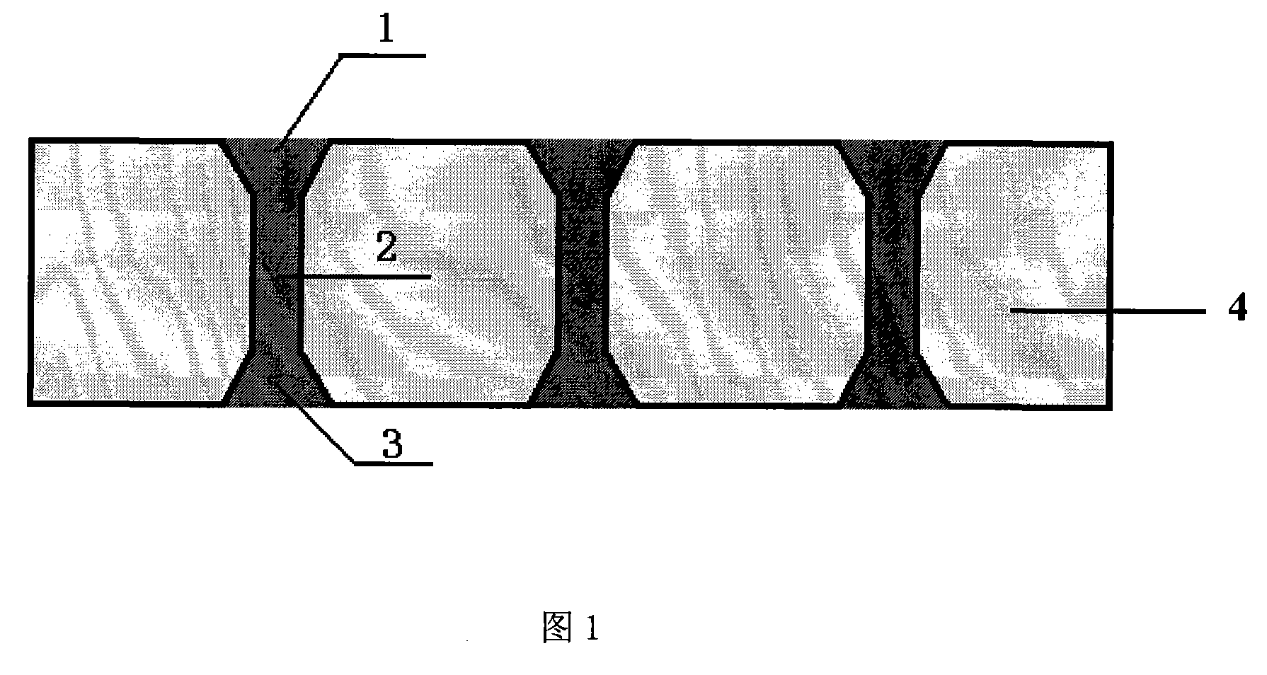
Figure 1 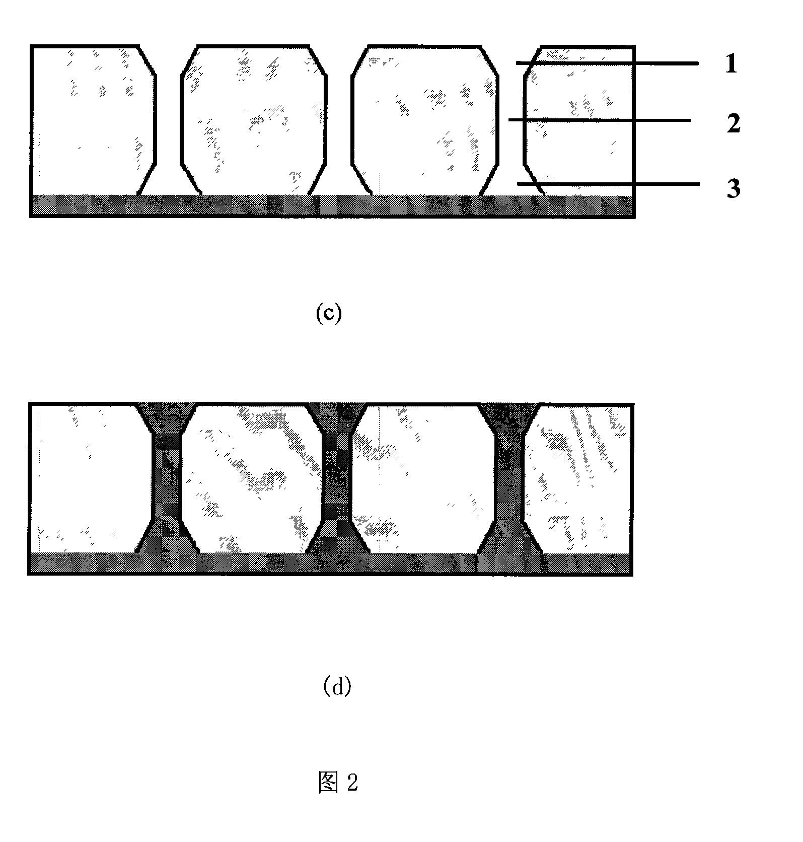
Figure 2 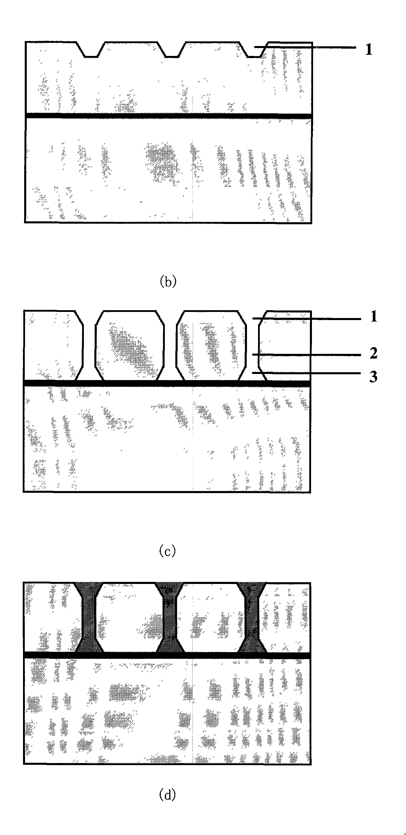
Figure 3
Abstract
Description
technical field
[0001] The invention relates to microelectronic packaging technology, in particular to a vertical interconnection via hole structure design and a preparation method for packaging and integrating low-frequency chips, radio frequency chips and MEMS chips. Background technique
[0002] The rapid development of current information technology and its application in the military and consumer markets has put forward new requirements for the system-level integration of microelectronic circuits and MEMS (micro-electromechanical systems), mainly including: the ability to acquire and store massive multimedia information, Accurately and reliably process and transmit these information at extremely high speed, and display useful information or use it for control in a timely manner. The development of integrated circuits in terms of integration has always followed "Moore's Law", but now with the integration of integrated circuit technology into the 65nm technology platform,...
Examples
Embodiment 1
[0042] Embodiment 1. The vertical interconnection via holes are prepared on the silicon chip on which the flash memory circuit has been fabricated.
[0043] The steps are shown in Figure 2, including:
[0044] 1. Select silicon wafers with flash memory circuits or other integrated circuits, as shown in Figure 2(a), and carry out carrier bonding;
[0045] 2. Protect the circuit part on the silicon wafer, and use a mask to perform the first DRIE via etching with a dip angle at the position where the vertical via hole connection in the silicon wafer is required to form the upper conical part of the via hole. Among them, SF 6Gas flow rate 130sccm, C 4 f 8 The gas flow rate is 100 sccm, the power of the slide stage is 13W, the power of the coil is 600W, and the APC (automatic pressure control) is selected as 60. After every 6s of etching, passivation is performed for 9s, and the etching and passivation are alternately performed to form sidewalls with slopes and depths that meet...
Embodiment 2
[0051] Embodiment 2: Vertical interconnection via holes are prepared on the SOI wafer.
[0052] refer to image 3 , whose steps include:
[0053] 1. Select SOI silicon wafer, such as image 3 as shown in (a);
[0054] Protect the circuit part of the device layer on the silicon wafer, and use a mask to perform the first DRIE via hole etching with an angle at the position where the vertical via hole connection is required in the silicon wafer, and make the upper end angle of the required size. The reference data is SF 6 Gas flow rate 130sccm, C 4 f 8 The gas flow rate is 100 sccm, the power of the slide stage is 13W, the power of the coil is 600W, and the APC (automatic pressure control) is selected as 60. Passivation for 9s after each etching for 6s, etching and passivation are performed alternately, and finally form a sidewall with a slope, such as image 3 as shown in (b);
[0055] 2. Adjust the mask for the vertical via holes in the etched silicon wafer, and perform the...
Embodiment 3
[0063] Embodiment 3: A standard silicon wafer with an integrated circuit processed on the upper surface is prepared for vertical interconnection via holes.
[0064] refer to Figure 4 , whose steps include:
[0065] 1. Protect the circuit part on the silicon chip, and use a mask to perform the first DRIE via hole etching with an inclination angle at the position where the vertical via hole connection in the silicon chip is required, and make the upper end inclination angle of the required size; refer to the data for SF 6 Gas flow rate 130sccm, C 4 f 8 The gas flow rate is 100 sccm, the power of the slide stage is 13w, the power of the coil is 600w, and the APC (automatic pressure control) is selected as 60. After etching for 6s, passivate for 9s to form sidewalls with slopes, such as Figure 4 as shown in (a);
[0066] 2. Add silicon carrier protection on the upper surface of the silicon wafer, such as Figure 4 As shown in (b); and thinning the back, such as Figure 4...