
I/O (input/output)pin allotting method for nano CMOS (Complementary Metal-Oxide-Semiconductor Transistor) circuit structure
A technology of circuit structure and distribution method, applied in circuits, electrical components, electrical digital data processing, etc., can solve problems such as skyrocketing manufacturing costs, hindering signal integrity, and serious wiring crosstalk.
Patent Information
- Authority / Receiving Office
- CN · China
- Current Assignee / Owner
- Publication Date
- 2011-06-22
- Estimated Expiration
- Not applicable · inactive patent
Smart Images
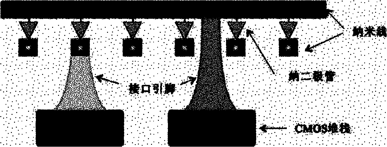
Figure 1 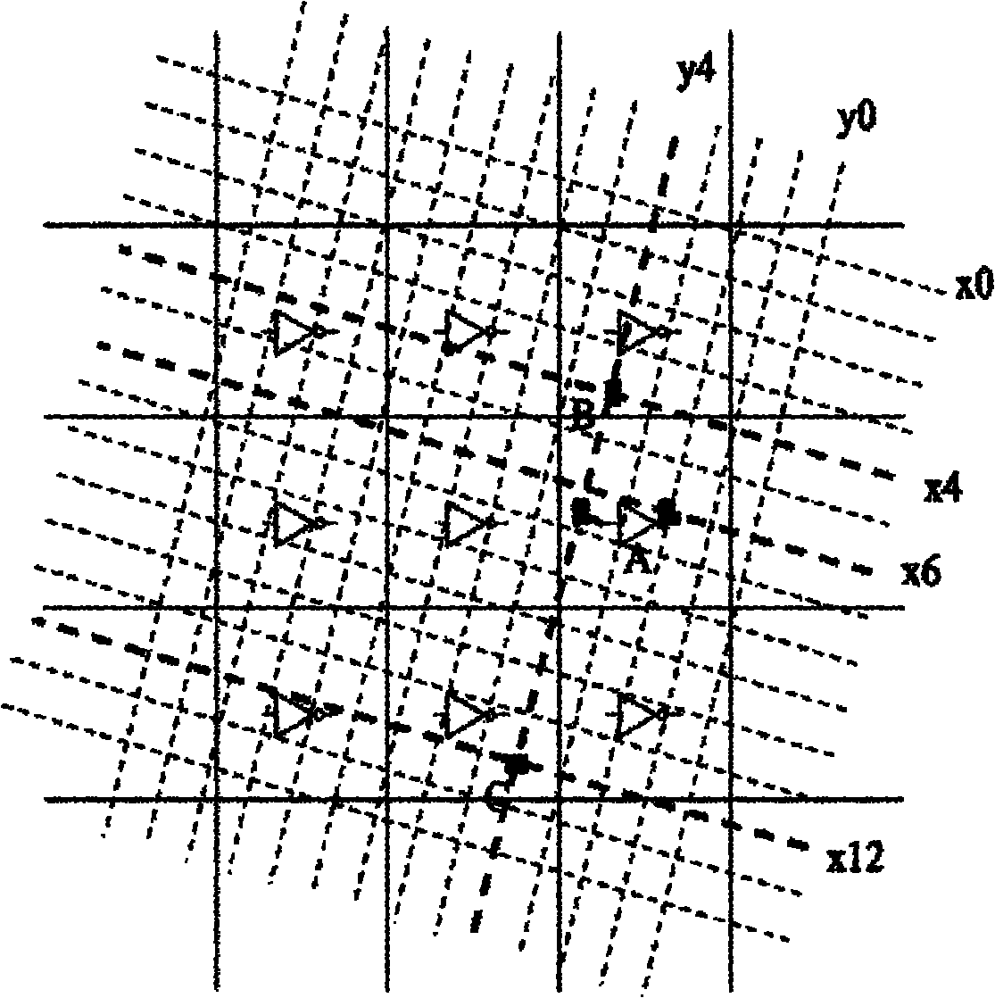
Figure 2 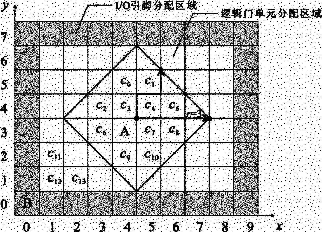
Figure 3
Abstract
Description
technical field
[0001] The invention relates to an automatic design method for a nanometer CMOS circuit structure, in particular to an I / O pin assignment method for a nanometer CMOS circuit structure. Background technique
[0002] At present, the large-scale production technology of silicon-based integrated circuits has reached the 0.09~0.065 micron process, and will further reach 0.045 micron or even reach the nanometer level. With the further narrowing of the line width of integrated circuits, silicon-based microelectronics technology will encounter many insurmountable challenges: (1) The difficulty of controlling line width through photolithography has increased sharply, which has far exceeded the current manufacturing level, making the development of corresponding The cost of manufacturing tools skyrocketed. (2) The quantum effect makes the crosstalk between the wires increasingly serious, hindering the integrity of the signal. For these reasons, silicon-based microele...
Examples
Embodiment 1
[0039] Embodiment one: step 1.: define the circuit netlist and include I / O pin, logic gate unit and interconnection line, take as Figure 6 The netlist of the input circuit based on the NOR gate is shown, and the I pin and the O pin in the input circuit netlist are saved separately to the collection , in, then , , the total number of I / O pins is , save the logic gate units in the input circuit netlist to the set G, then , the number of logic gate units is ;
[0040] Step ②: Define the nano-CMOS circuit structure as a two-dimensional cell array , whose size is , the horizontal coordinates are , the vertical coordinate is ,in is a nano-CMOS unit, that is, the number of nano-CMOS units ; The outermost nano-CMOS unit of the two-dimensional cell array is an I / O pin allocation area, and the remaining nano-CMOS cells of the two-dimensional cell array are logic gate cell allocation areas; in the formula (2) is the redundant control parameter, The value is 2...
Embodiment 2
[0045] Step ①: Define the circuit netlist including I / O pins, logic gate units and interconnection lines, such as Figure 9 The netlist of the input circuit based on the NOR gate is shown, and the I pin and the O pin in the input circuit netlist are saved separately to the collection , in, then , , the total number of I / O pins is . Save the logic gate units in the input circuit netlist to the set G, , the number of logic gates is ;
[0046] Step ②: Define the nano-CMOS circuit structure as a two-dimensional cell array , whose size is , the horizontal coordinates are , the vertical coordinate is ,in is a nano-CMOS unit, that is, the number of nano-CMOS units ; The outermost nano-CMOS unit of the two-dimensional cell array is an I / O pin allocation area, and the remaining nano-CMOS cells of the two-dimensional cell array are logic gate cell allocation areas; in the formula (2) is the redundant control parameter, The value is 40; according to formulas ...