
Microelectronic packages and associated methods of manufacturing
A technology of microelectronic packaging and manufacturing methods, which is applied in the direction of circuits, electrical components, and electrical solid devices, can solve the problems of solder ball collapse, difficult operation, time-consuming, etc., and achieve the effect of controlling collapse
Patent Information
- Authority / Receiving Office
- CN · China
- Patent Type
- Applications(China)
- Current Assignee / Owner
- Publication Date
- 2012-06-27
- Estimated Expiration
- Not applicable · inactive patent
Smart Images
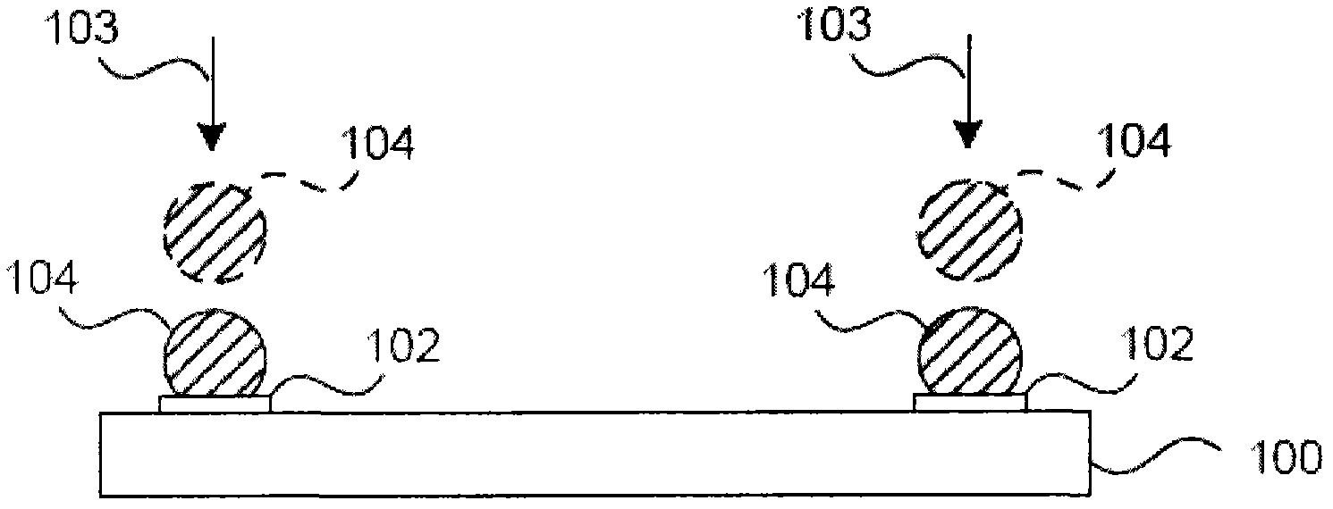
Figure 1 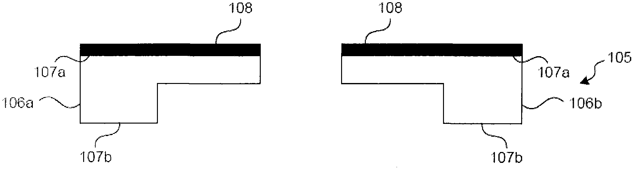
Figure 2 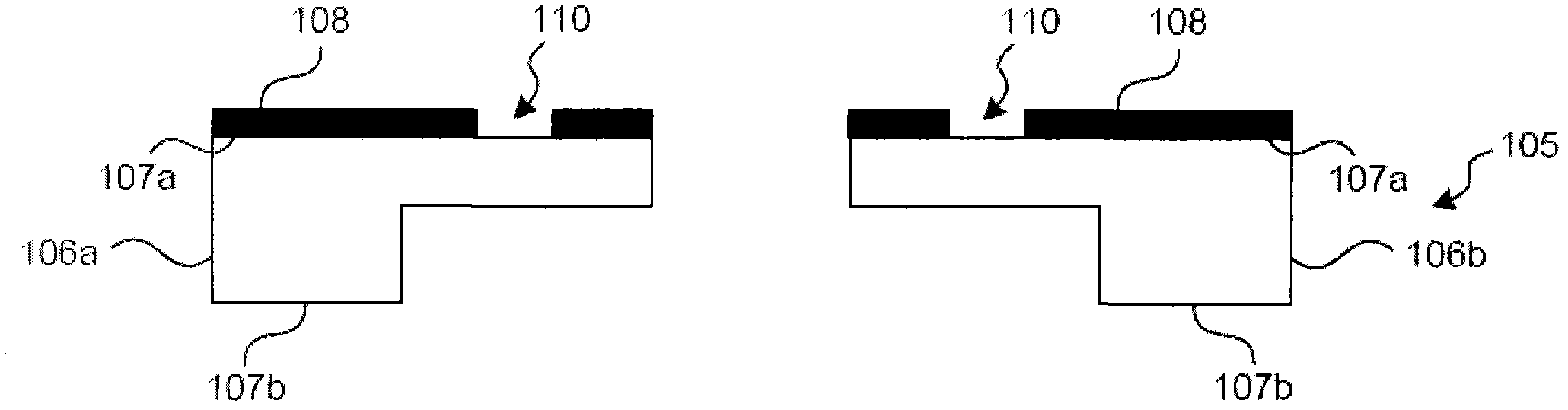
Figure 3
Abstract
Description
technical field
[0001] The invention relates to an electronic component, in particular to a microelectronic package and a manufacturing method thereof. Background technique
[0002] Flip-chip technology is a technology that directly connects a semiconductor chip to a substrate through solder balls or solder bumps. In the packaging process, the solder balls are first placed on the semiconductor chip, and a solder mask is formed on the substrate (such as a printed circuit board) to determine multiple connection points, and then the semiconductor chip with the solder balls attached is turned over and the solder The balls are aligned to the corresponding connection points on the substrate, and the connections are finally reflowed.
[0003] A disadvantage of the flip-chip technique described earlier is that when the substrate is a lead frame with multiple pins, the solder balls may collapse uncontrollably during reflow. Uncontrolled solder ball collapse may result in structural...
Examples
Embodiment Construction
[0015] Embodiments of the present invention are described below with reference to the drawings. A package packaged with a semiconductor chip is called a microelectronic package. Usually, a microelectronic package provides protection, power supply, and cooling for the internal chip and related components while minimizing the impact on the electrical performance of the semiconductor chip, and provides electrical and external connections. and mechanical contact. A typical microelectronic package includes microelectronic circuits or components, thin film recording heads, data storage units, microfluidic devices, and other components formed on microelectronic substrates. Microelectronic substrates may include semiconductor substrates (such as wafers doped with silicon or gallium arsenide), insulating sheets (such as ceramic substrates), or conductive sheets (such as metals or metal alloys). The "semiconductor chip" referred to herein may include products used in various situations...