
Compensation method for increase of amplification times of direct current caused by thinning of germanium-silicon edge
A technology of DC current and compensation method, applied in the manufacturing of circuits, electrical components, semiconductor/solid-state devices, etc., can solve problems such as yield drop, achieve yield improvement, compensate for the rise of collector current, and tighten the distribution of magnification. Effect
Patent Information
- Authority / Receiving Office
- CN · China
- Patent Type
- Patents(China)
- Current Assignee / Owner
- Publication Date
- 2015-06-03
Smart Images
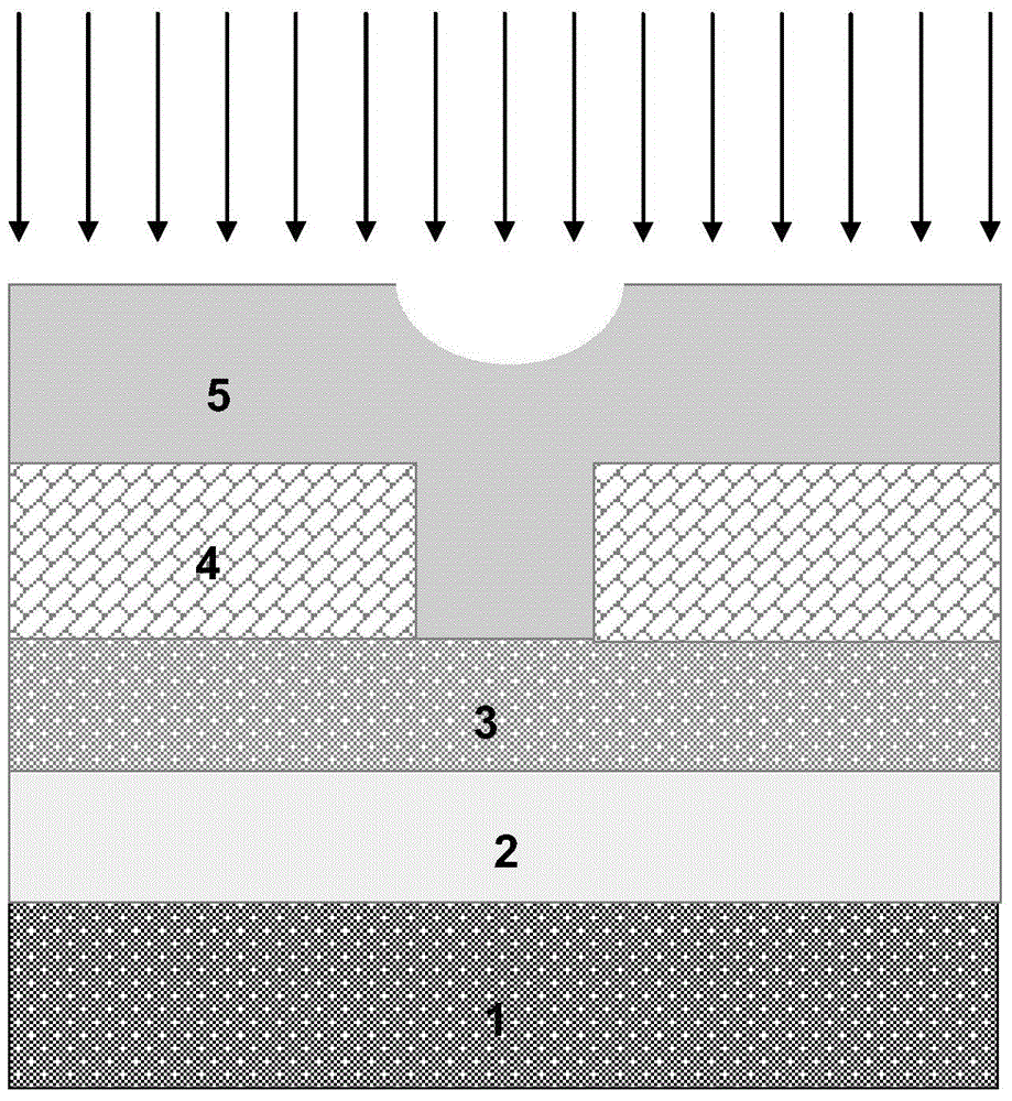
Figure 1 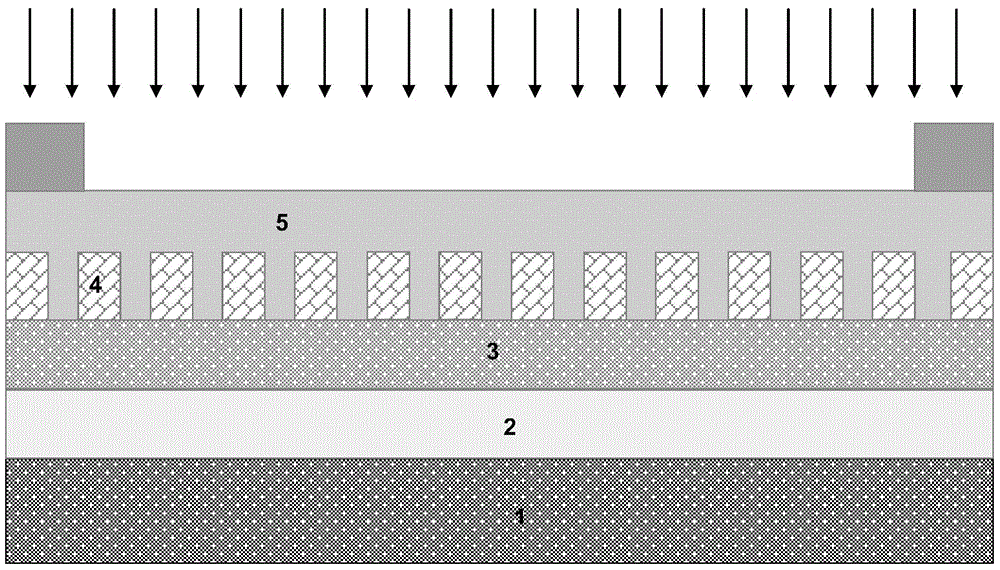
Figure 2 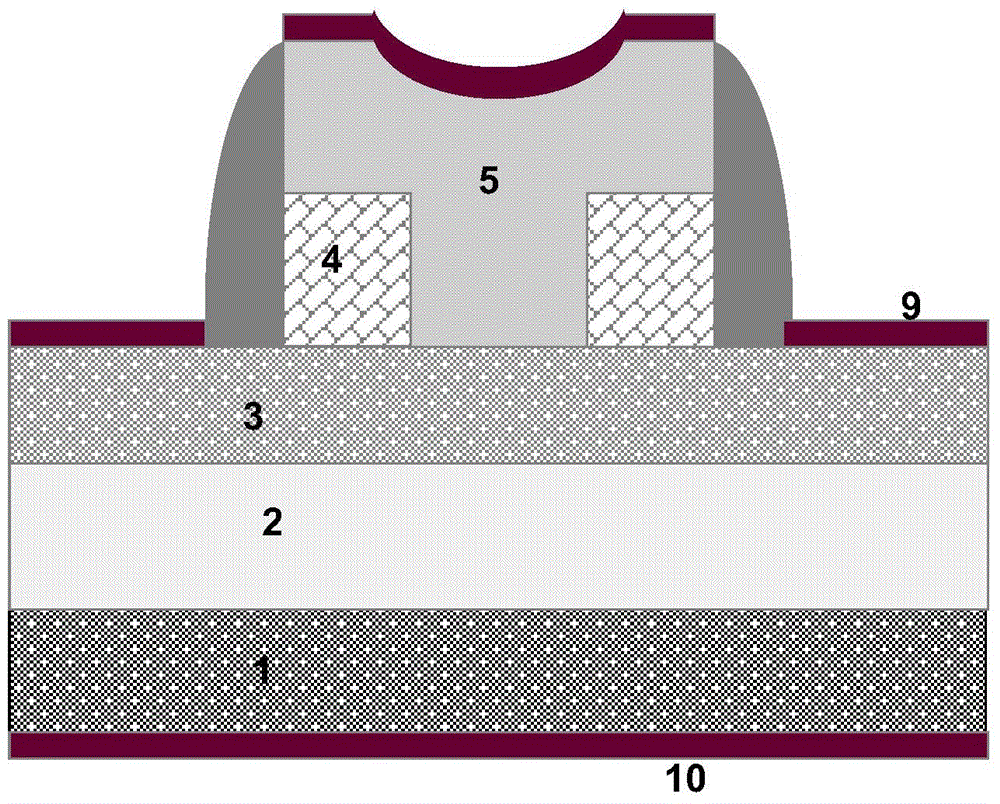
Figure 3
Abstract
Description
technical field
[0001] The invention relates to the field of semiconductor integrated circuits, in particular to a method for compensating the increase in collector current caused by edge thinning when germanium and silicon are grown on a non-patterned optical sheet in the manufacturing process of germanium-silicon heterojunction bipolar triode power devices The method of multiplying the dc current method caused by it. Background technique
[0002] For radio frequency applications in the 1G Hz range, germanium-silicon heterojunction bipolar transistor devices generally adopt the method of leading out the collector on the back, that is, low N-doped epitaxial growth is performed on the N-type heavily doped substrate to form the collector region. Its advantage is that the process is simple, and the mask layer can be reduced by half compared with the traditional process. The disadvantage is that when silicon germanium is grown on the optical wafer, the thickness of the silicon g...
Examples
Embodiment Construction
[0024] The compensation method for increasing the direct current amplification factor caused by the thinning of the silicon germanium edge of the present invention is mainly used in the manufacturing process of the emitter area, and the manufacturing process of the collector area and the base area is the same as the commonly used manufacturing process, such as Figure 4 shown. The collector region is manufactured by growing a low N-doped epitaxial layer 2 on a heavily doped N-type silicon substrate 1, with a thickness between 1.0 and 5.0 microns and a doping concentration of 10 15 ~10 17 cm -3 . The manufacture of the base area is to grow a silicon-germanium epitaxial layer 3 on the N-type epitaxial layer 2. The silicon-germanium epitaxial layer 3 is divided into three layers: a silicon buffer layer, a silicon-germanium layer, and a silicon cap layer. Among them, the silicon-germanium layer has a highly doped doped boron and the silicon cap layer has low doped boron. The t...