
A kind of gan-based enhanced hemt device and its preparation method
An enhanced device technology, applied in semiconductor/solid-state device manufacturing, semiconductor devices, electrical components, etc., can solve problems such as low threshold voltage, reduced gate control capability, and current collapse, so as to reduce design difficulty and cost, Achieving enhanced device effects
Patent Information
- Authority / Receiving Office
- CN · China
- Patent Type
- Patents(China)
- Current Assignee / Owner
- Publication Date
- 2017-07-14
- Estimated Expiration
- Not applicable · inactive patent
Smart Images
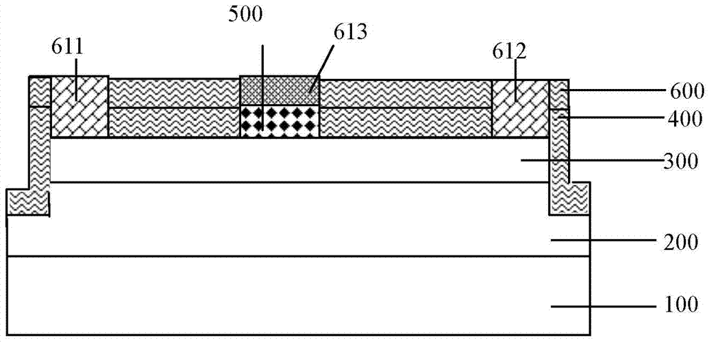
Figure 1 
Figure 2 
Figure 3
Abstract
Description
technical field
[0001] The invention relates to the field of manufacturing semiconductor devices, in particular to a GaN-based enhanced HEMT device and a preparation method thereof, in which a novel p-type multi-element nitride alloy with gradual composition is added to a GaN heterojunction structure. Background technique
[0002] GaN material has unique advantages in the preparation of high-voltage, high-temperature, high-power and high-density integrated electronic devices because of its large band gap, high critical breakdown electric field, and high thermal conductivity.
[0003] GaN materials can form heterojunction structures with AlGaN, InAlN and other materials. Due to the spontaneous polarization and piezoelectric polarization effects of barrier layer materials such as AlGaN or InAlN, a high-concentration and high-mobility two-dimensional electron gas (2DEG) will be formed at the heterojunction interface. This characteristic can not only improve the carrier mobilit...
Examples
Embodiment Construction
[0037] In order to make the object, technical solution and advantages of the present invention clearer, the present invention will be described in further detail below in conjunction with specific embodiments and with reference to the accompanying drawings.
[0038] figure 1 It is a schematic structural diagram of a GaN-based enhancement mode HEMT device according to an embodiment of the present invention, such as figure 1 As shown, in an embodiment of the present invention, the GaN-based enhanced HEMT device includes: a substrate 100, a GaN intrinsic layer 200, a barrier layer 300, a high hole concentration structure layer 500, a first metal electrode 611, a second The second metal electrode 612, the third metal electrode 613, the passivation medium layer 400 and the passivation protection layer 600, wherein:
[0039] The GaN intrinsic layer 200 and the barrier layer 300 are sequentially grown on the substrate 100;
[0040] The high hole concentration structure layer 500 co...