
Thin film transistor and manufacturing method and organic light emitting diode display device thereof
A thin-film transistor and light-emitting diode technology, which is applied in the direction of transistors, semiconductor/solid-state device manufacturing, semiconductor devices, etc., can solve the problems of significant floating body effect, inability to effectively suppress the floating body effect, and increase in the area of thin-film transistors, so as to suppress the floating body effect and improve Electrical characteristics, the effect of increasing the area
Patent Information
- Authority / Receiving Office
- CN · China
- Patent Type
- Patents(China)
- Current Assignee / Owner
- Publication Date
- 2018-05-22
Smart Images
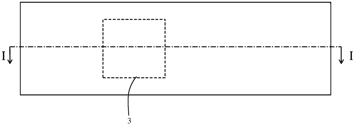
Figure 1 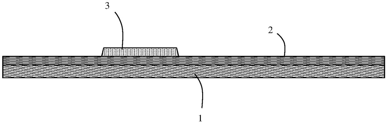
Figure 2 
Figure 3
Abstract
Description
technical field
[0001] The invention relates to the field of display technology, in particular to a thin film transistor, a manufacturing method and an organic light emitting diode display device thereof. Background technique
[0002] Organic light-emitting diode (OLED) display device is an active light-emitting device. Compared with the current mainstream flat-panel display technology thin-film transistor liquid crystal display (TFT-LCD), OLED has the advantages of high contrast, wide viewing angle, low power consumption, and thinner volume. , is expected to become the next-generation flat panel display technology after LCD, and is one of the most concerned technologies in flat panel display technology, especially suitable for large-sized active matrix organic light emitting diode (Active Matrix OLED, AMOLED) display devices. Polycrystalline silicon (poly-Si) with higher mobility is widely used as thin film transistors due to the large demand for driving current in OLEDs an...
Examples
Embodiment Construction
[0046] Figure 1A A plan view showing the first step of a method of manufacturing a TFT according to an exemplary embodiment of the present invention, Figure 1B for along Figure 1A A cross-sectional view taken along the line I-I. see Figure 1A with 1B A substrate 1 is provided, the substrate 1 is formed of glass or plastic, and a buffer layer 2 is formed on the substrate 1, and the buffer layer 2 is formed on the substrate 1 by chemical vapor deposition (CVD). The buffer layer 2 functions to prevent moisture or impurities in the substrate from diffusing into the semiconductor layer, or to control heat transfer efficiency during crystallization to facilitate crystallization of the semiconductor layer, which will be formed in the following process. The buffer layer 2 can be a single layer, or can be composed of multi-layer films.
[0047] Subsequently, a first amorphous silicon layer is formed on the buffer layer 2 . It can be formed by chemical vapor deposition (CVD), and...