
A manufacturing method for a groove type super junction
A manufacturing method and super junction technology, applied in semiconductor/solid-state device manufacturing, electrical components, circuits, etc., can solve problems such as poor reverse breakdown voltage uniformity, and achieve the effect of improving in-plane uniformity
Patent Information
- Authority / Receiving Office
- CN · China
- Current Assignee / Owner
- Publication Date
- 2016-06-22
Smart Images
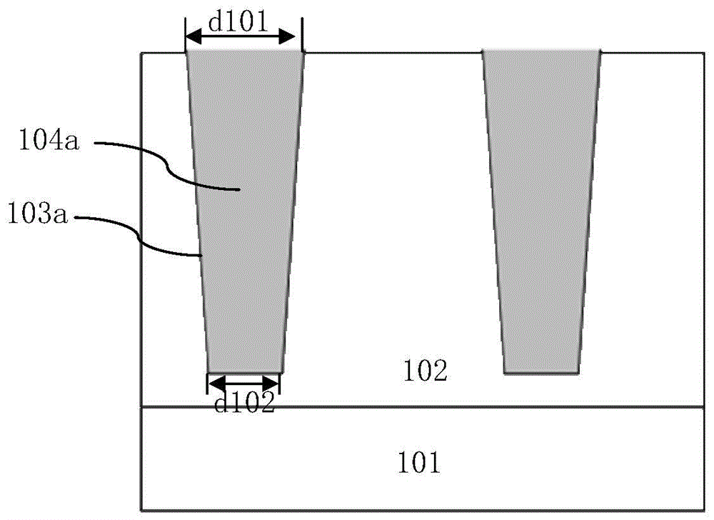
Figure 1 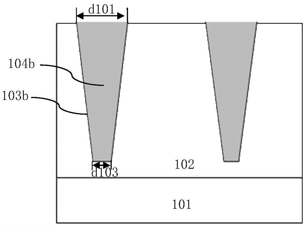
Figure 2 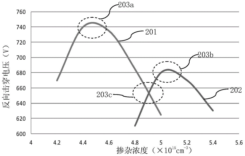
Figure 3
Abstract
Description
technical field
[0001] The invention relates to a manufacturing process method of a semiconductor integrated circuit, in particular to a manufacturing method of a trench type super junction. Background technique
[0002] The super junction is composed of alternately arranged P-type thin layers and N-type thin layers formed in the semiconductor substrate, and the depletion layer formed by matching the P-type thin layers and N-type thin layers is used to support the reverse withstand voltage. The existing super junction manufacturing method includes the manufacturing method of trench type super junction. This method is to manufacture super junction devices through trench technology. Etch a trench with a certain depth and width, and then fill the etched trench with P-type doped silicon epitaxy by means of epitaxial filling (ERIFilling). In the etching of trenches, the morphology of trenches in different regions of the same semiconductor substrate wafer is not completely the sa...
Examples
Embodiment Construction
[0032] Such as Figure 1A As shown, it is a schematic diagram of the structure of a super junction located in the edge region of the wafer formed by the existing trench-type super junction manufacturing method; as Figure 1B Shown is a schematic diagram of the structure of the super junction located in the middle region of the wafer formed by the existing trench-type super junction manufacturing method; the existing trench-type super junction manufacturing method includes the following steps:
[0033] Step 1. Provide a semiconductor substrate wafer 101, on the surface of the semiconductor substrate wafer 101, a first conductivity type epitaxial layer 102 is formed, and the N-type epitaxial layer 102 is taken as an example for illustration below;
[0034] Step 2, using a photolithography process to define a trench formation area and open the trench formation area; in the existing method, the size of the trenches at different positions on the semiconductor substrate wafer 101 is ...