
Groove power device with buried layer and manufacturing method thereof
A manufacturing method and technology of power devices, which are applied in semiconductor/solid-state device manufacturing, semiconductor devices, electrical components, etc., and can solve problems such as increased on-resistance
Patent Information
- Authority / Receiving Office
- CN · China
- Current Assignee / Owner
- Publication Date
- 2016-11-23
- Estimated Expiration
- Not applicable · inactive patent
Smart Images
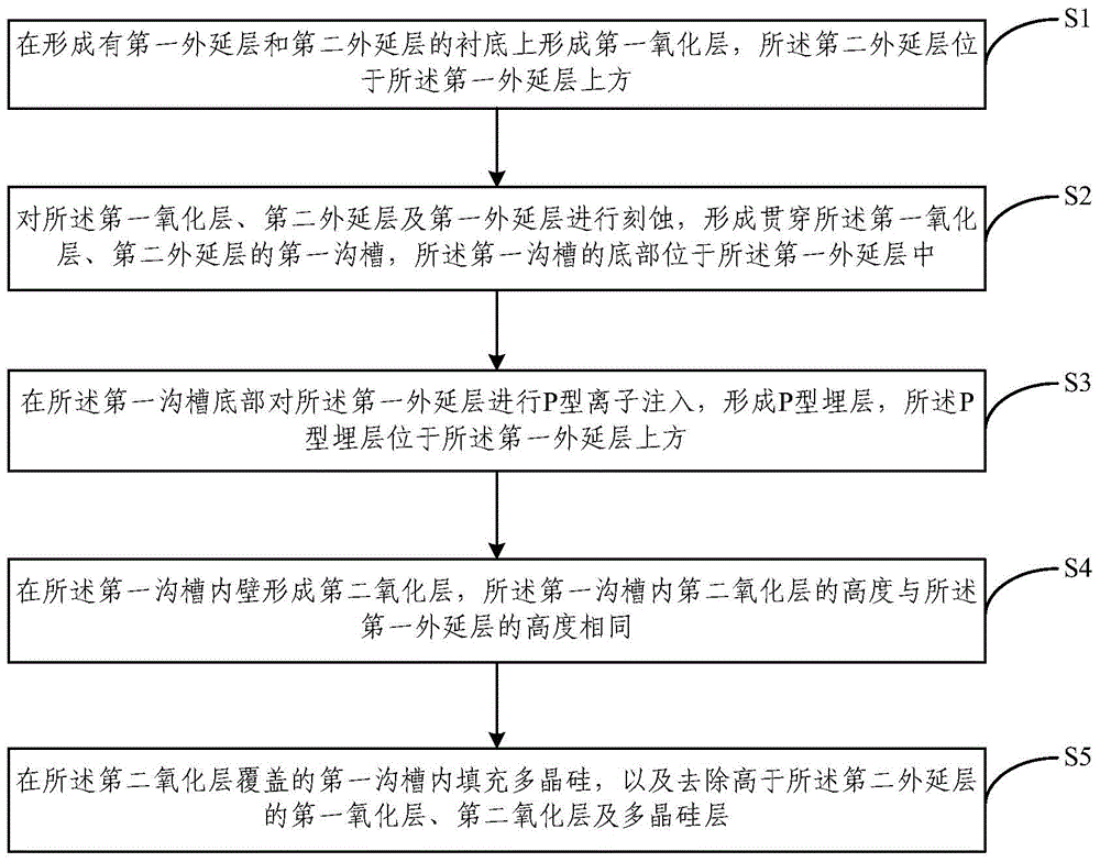
Figure 1 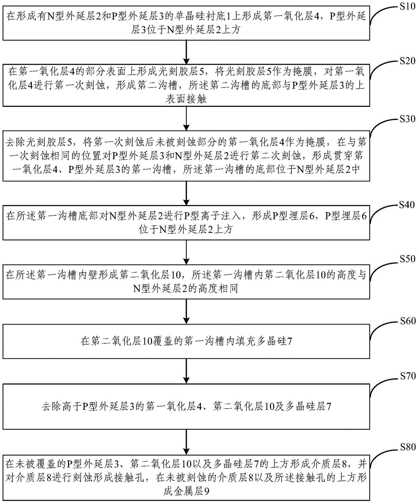
Figure 2 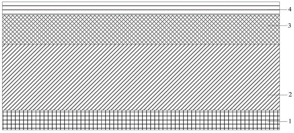
Figure 3
Abstract
Description
technical field
[0001] The invention relates to the technical field of semiconductors, in particular to a trench power device with a buried layer and a manufacturing method thereof. Background technique
[0002] Trench type Vertical Double Diffused Metal Oxide Semiconductor (VDMOS) transistors combine the advantages of bipolar transistors and ordinary Metal Oxide Semiconductor (MOS) devices, whether it is switching applications or linear applications , VDMOS is an ideal power device. The drain and source poles of VDMOS are on both sides of the device, so that the current flows vertically inside the device, which increases the current density and improves the rated current. The on-resistance per unit area is also small, which is A very versatile power device.
[0003] In the design process of trench power devices, the contradiction between breakdown voltage and on-resistance is the bottleneck of device performance improvement. The breakdown point of the trench power device ...
Examples
no. 1 example
[0050] figure 1 The method for fabricating the buried trench power device provided by the first embodiment of the present invention is shown, as figure 1 As shown, the manufacturing method of the power device with a buried trench provided by the first embodiment of the present invention is as follows.
[0051] S1. Form a first oxide layer on a substrate formed with a first epitaxial layer and a second epitaxial layer, the second epitaxial layer is located above the first epitaxial layer.
[0052] In a specific application, the first epitaxial layer is an N-type epitaxial layer, and the second epitaxial layer is a P-type epitaxial layer.
[0053] In a specific application, the substrate of the present embodiment and / or the matrix of the first epitaxial layer and / or the second epitaxial layer may be single crystal silicon or the like.
[0054]S2. Etching the first oxide layer, the second epitaxial layer, and the first epitaxial layer to form a first trench penetrating through ...
no. 2 example
[0078] In order to more clearly illustrate the technical solutions of the embodiments of the present invention, a more specific embodiment is given below, figure 2 It shows a schematic flowchart of a method for fabricating a power device with a buried trench provided by the second embodiment of the present invention, as shown in figure 2 As shown, in this embodiment, single crystal silicon is used as the substrate, and the method for manufacturing a power device with a buried trench provided by the second embodiment of the present invention is as follows.
[0079] S10, forming a first oxide layer 4 on the single crystal silicon substrate 1 formed with an N-type epitaxial layer 2 and a P-type epitaxial layer 3, and the P-type epitaxial layer 3 is located above the N-type epitaxial layer 2, such as image 3 shown.
[0080] It should be noted that the selection of the substrate material mainly depends on the following aspects: structural properties, interface properties, chemi...
no. 3 example
[0095] This embodiment provides a power device with a buried trench, and the power device with a buried trench is manufactured using the manufacturing method described in the first or second embodiment.
[0096] In the trench power device with a buried layer in this embodiment, the P-type buried layer in the N-type drift region can increase the withstand voltage of the depletion layer of the trench power device, and can reduce the on-resistance of the device under the same withstand voltage. The second oxide layer can improve the withstand voltage capability at the corner at the bottom of the trench, and greatly improve the breakdown characteristics of the device.