
Electrooptical adjustable filter based on sub-wavelength high-contrast grating
A high-contrast grating and sub-wavelength grating technology, applied in the field of optoelectronics, can solve the problems of short tuning time, large driving voltage, low transmittance, etc., and achieve the effects of short tuning time, reducing driving voltage and increasing tuning rate.
Patent Information
- Authority / Receiving Office
- CN · China
- Patent Type
- Applications(China)
- Current Assignee / Owner
- Publication Date
- 2017-08-18
Smart Images
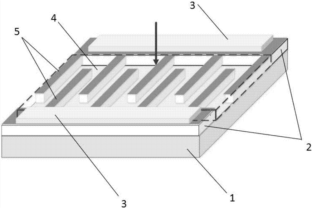
Figure 1 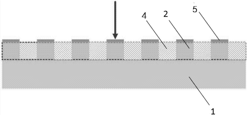
Figure 2 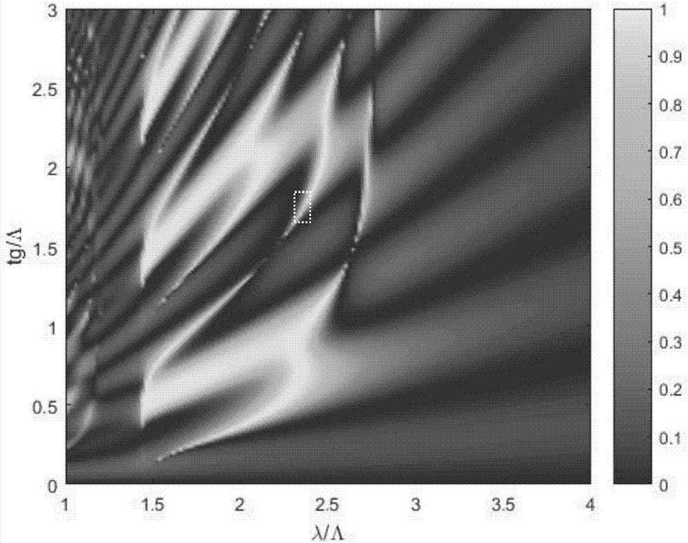
Figure 3
Abstract
Description
technical field
[0001] The invention belongs to the technical field of optoelectronics, and specifically relates to a filter capable of realizing the adjustable filtering function of the optical communication band through an external voltage. Background technique
[0002] In today's digital age, optical communication technology is developing at an unimaginable speed, and wavelength division multiplexing (Wavelength division multiplexer, WDM) has greatly increased the capacity of optical communication systems. With the application of wavelength division multiplexing (WDM) technology, optical communication technology has developed rapidly. In the future, optical communication technology will develop in a more intelligent and efficient direction. As a key device in wavelength division multiplexing technology, tunable optical filters have received more and more attention and research. The tunable optical filter is a wavelength selection device, and its function is to select an ...
Examples
Embodiment 1
[0040] In this embodiment, the simulation parameters are set as follows: in this embodiment, the material of the substrate 1 is silicon dioxide, and the material of the grating 2 is silicon; the grating period Λ is 650 nm, the duty ratio is 0.5, and the grating thickness is 1100 nm; The refractive index of the substrate material is 3.48, the refractive index of the substrate material is 1.44, and the refractive index of the electro-optic material layer material n 0 (when the driving voltage is zero) is 1.60.
[0041] In this embodiment, TM polarized light is incident, and since the thickness of the transparent conductive layer 5 is very small, the influence of the thickness of the transparent conductive layer 5 can be ignored in the simulation process. In this embodiment, the strict coupled wave analysis method is used for simulation, and Matlab simulation software is used to draw the following image 3 Reflectance contour plot of the shown electro-optic tunable filter based ...
Embodiment 2
[0045] In this embodiment, the simulation parameters are set as follows: in this embodiment, the material of the substrate 1 is silicon dioxide, and the material of the grating 2 is silicon; the grating period Λ is 650 nm, the duty ratio is 0.5, and the grating thickness is 1100 nm; The refractive index of the substrate material is 3.48, the refractive index of the substrate material is 1.44, and the refractive index of the electro-optic material layer material is 1.65 (the driving voltage is not zero at this time); the electro-optic material selects the electro-optic coefficient r 33 300pm / V electro-optic polymer.
[0046] In this embodiment, TM polarized light is used for incident, and the simulation is carried out according to the strict coupled wave analysis method, and the following is obtained by using Matlab simulation software to draw Figure 5 The reflectance spectrum is shown, in which, the small picture in the upper right corner is an enlarged view of the reflectanc...
Embodiment 3
[0052] In this embodiment, the simulation parameters are set as follows: in this embodiment, the material of the substrate 1 is silicon dioxide, and the material of the grating 2 is silicon; the grating period Λ is 650 nm, the duty ratio is 0.5, and the grating thickness is 1100 nm; The refractive index of the substrate material is 3.48, the refractive index of the substrate material is 1.44, and the refractive index of the electro-optic material layer material is 1.70 (the driving voltage is not zero at this time); the electro-optic material selects the electro-optic coefficient r 33 300pm / V electro-optic polymer.
[0053] In this embodiment, TM polarized light is used for incident, and the simulation is carried out according to the strict coupled wave analysis method, and the following is obtained by using Matlab simulation software to draw Figure 6 The reflectance spectrum is shown, in which, the small picture in the upper right corner is an enlarged view of the reflectanc...