
Wafer electroplating device and electroplating method
An electroplating device and wafer technology, applied in the direction of electrodes, circuits, electrolysis process, etc., can solve problems such as uneven thickness of electroplating layer, and achieve the effect of reducing the difficulty of grinding
Patent Information
- Authority / Receiving Office
- CN · China
- Current Assignee / Owner
- Publication Date
- 2021-05-25
- Estimated Expiration
- Not applicable · inactive patent
Smart Images
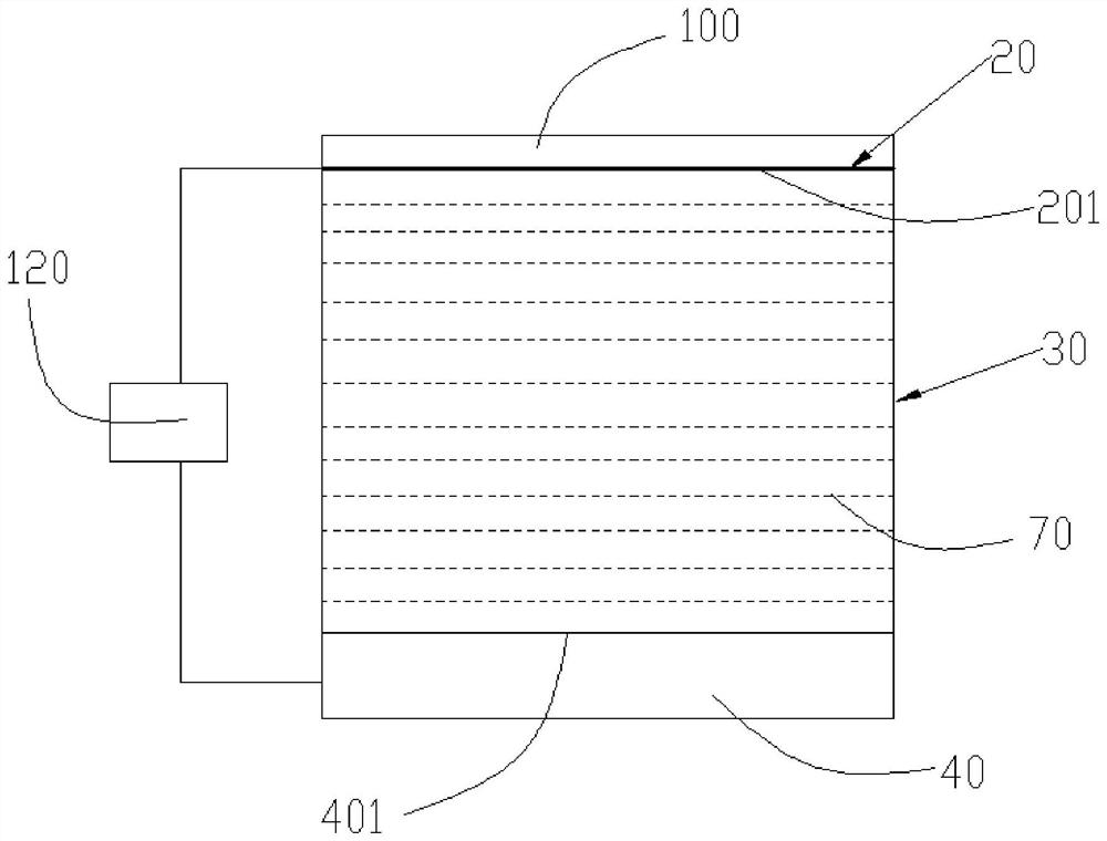
Figure 1 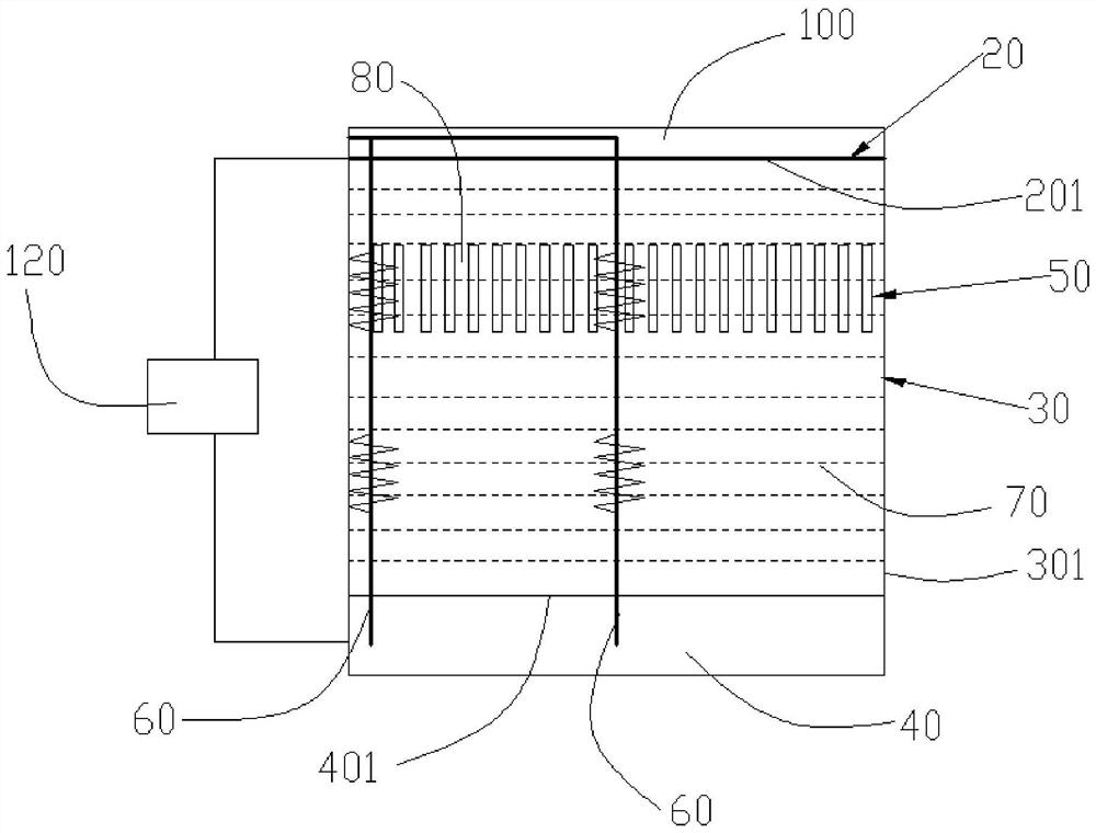
Figure 2 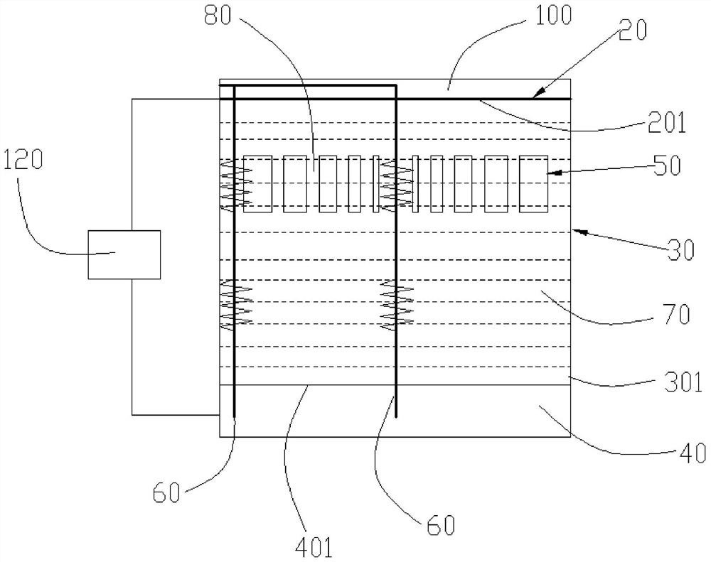
Figure 3
Abstract
Description
technical field
[0001] The invention relates to the technical field of semiconductor devices, in particular to a wafer electroplating device and an electroplating method. Background technique
[0002] At present, for the electroplating process (ECP) in semiconductors, since the power supply of electroplating is applied to the seed layer on the surface of the wafer, the seed layer on the surface of the wafer has a certain resistance, which makes the different positions of the seed layer Different currents on the seed layer will result in different thicknesses of the electroplating layer formed by electroplating at different positions of the final seed layer, which will increase the difficulty of subsequent grinding of the electroplating layer. Contents of the invention
[0003] The object of the present invention is to provide a wafer electroplating device and an electroplating method to solve the technical problem of uneven thickness of the electroplating layer formed by e...
Examples
Embodiment Construction
[0025] The following will clearly and completely describe the technical solutions in the embodiments of the present invention with reference to the accompanying drawings in the embodiments of the present invention. Obviously, the described embodiments are only some, not all, embodiments of the present invention. Based on the embodiments of the present invention, all other embodiments obtained by persons of ordinary skill in the art without creative efforts fall within the protection scope of the present invention.
[0026] Before describing the embodiments of the present invention, a conventional wafer 100 plating apparatus will be described first.
[0027] see figure 1 , the electroplating device of traditional wafer 100 comprises electroplating tank 30, electroplating anode 40 and power supply 120, is provided with electroplating solution 70 in electroplating tank 30, and the surface of wafer 100 is provided with seed layer 20, and electroplating anode 40 includes towards se...