
Circuit board tape and butt joint method thereof
A circuit and board roll technology, applied in the directions of printed circuit, printed circuit, printed circuit manufacturing, etc., can solve the problems of inability to carry out the process, the variation of the transmission hole distance, etc., and achieve the effect of the number of circuit layouts
Patent Information
- Authority / Receiving Office
- CN · China
- Patent Type
- Applications(China)
- Current Assignee / Owner
- Publication Date
- 2022-03-11
Smart Images
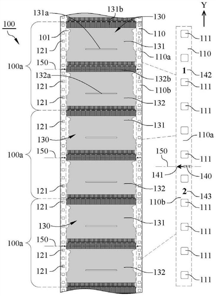
Figure 1 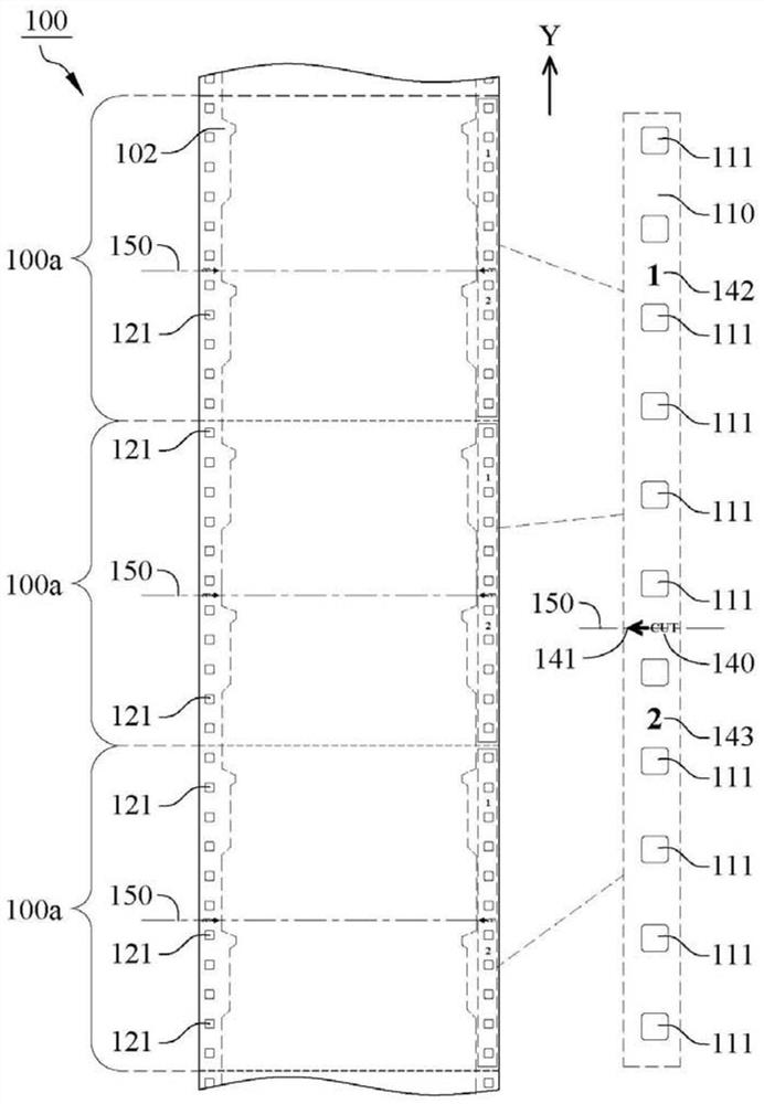
Figure 2 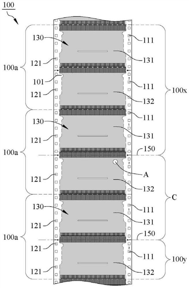
Figure 3
Abstract
Description
technical field
[0001] The invention relates to a circuit board tape and its docking method, in particular to a circuit board tape that can be docked after cutting unqualified substrate units and its docking method. Background technique
[0002] In the existing known circuit board tape design, a plurality of circuit layouts are arranged on the substrate, and a plurality of transmission holes are provided on both sides of the substrate, and each of the two sides of the circuit layout corresponds to an even number of transmission holes. And the pitch between the transmission holes must match the tooth pitch of the transmission member (such as a transmission wheel or a transmission bar), so that the transmission member can drive the substrate to carry out processes such as bonding wafers and gluing.
[0003] However, in the inspection step, the area with the unacceptable circuit layout is cut off, so that the circuit board reel is formed into a front reel and a rear reel, and t...
Examples
Embodiment Construction
[0044] see figure 1 and figure 2, a circuit board tape 100 of the present invention has a first surface 101 and a second surface 102, the circuit board tape 100 includes a plurality of substrate units 100a arranged along the transmission direction Y, each of the substrate units 100a has a first A transmission hole setting area 110, a second transmission hole setting area 120, a circuit layout area 130 and at least one docking mark 140, the first transmission hole setting area 110 has more than three first transmission holes 111 with an odd number, so The first transmission holes 111 are equidistantly arranged on one side of the substrate unit 100a, please refer to figure 1 and figure 2 In the partial enlarged view, in this embodiment, the first transmission hole setting area 110 has 11 first transmission holes 111 for illustration, but it is not limited thereto.
[0045] see figure 1 and figure 2 , the second transmission hole setting area 120 has more than three secon...