
Optical device, optical device apparatus, camera module, and optical device manufacturing method
A technology for optical equipment and optical components, used in radiation control devices, semiconductor/solid-state device manufacturing, electrical components, etc., can solve problems such as inability to prevent, limit the number of electrode terminals, and inability to prevent smearing or flashing, and achieve simple manufacturing. method, miniaturization, and effect of thinning
Patent Information
- Authority / Receiving Office
- CN · China
- Patent Type
- Applications(China)
- Current Assignee / Owner
- Publication Date
- 2007-01-24
- Estimated Expiration
- Not applicable · inactive patent
Smart Images
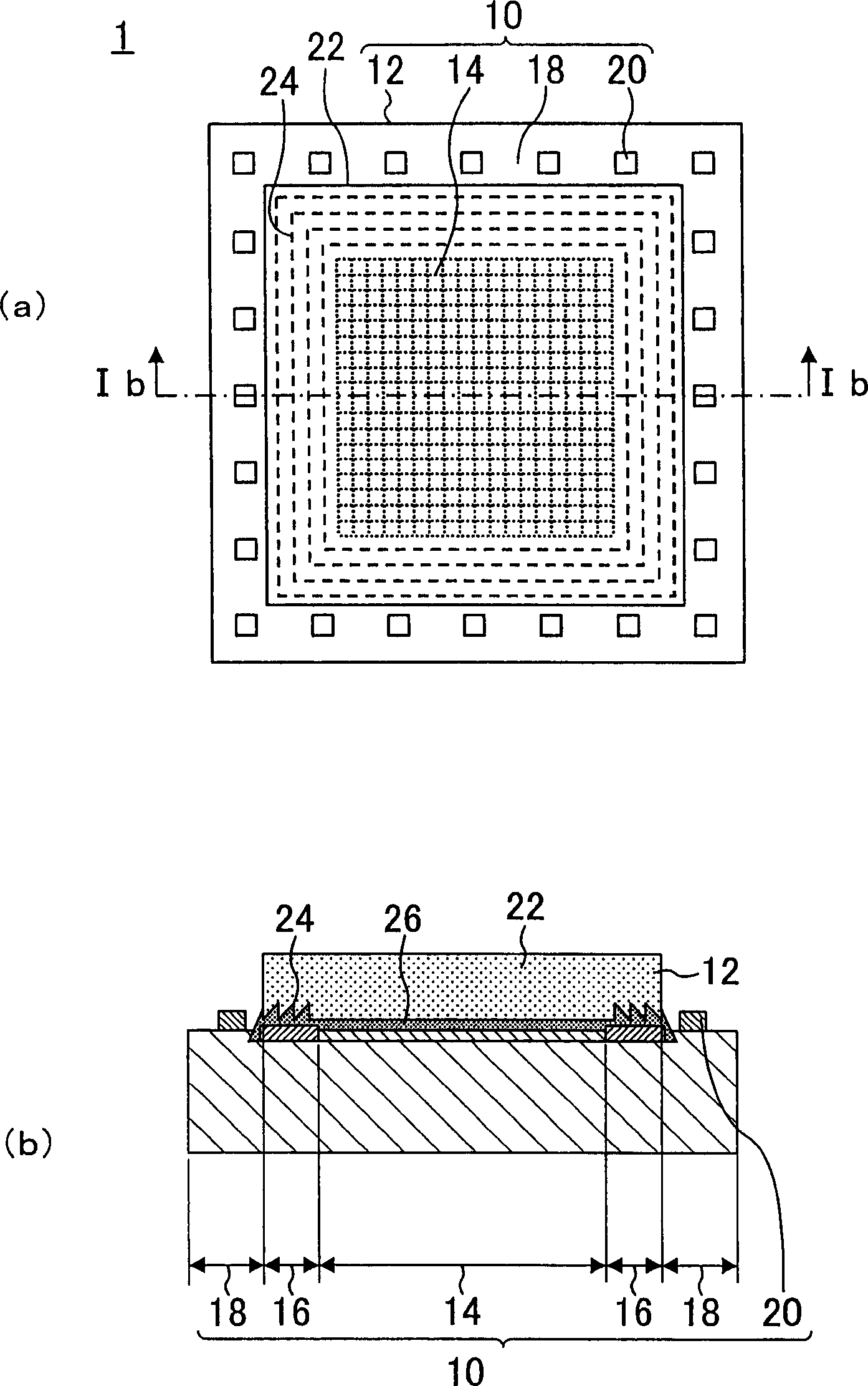
Figure 1 
Figure 2 
Figure 3
Abstract
Description
technical field
[0001] The present invention relates to an optical device and a method of manufacturing the same. Background technique
[0002] In recent years, with the development of miniaturization, thinning, light weight and high functionality of electronic equipment, the mainstream of semiconductor device mounting is shifting from the conventional packaging type mounting to the reverse mounting of bare chips or CSP structures on circuit boards, etc. installed. In semiconductor imaging devices, such a mounting configuration is also being studied.
[0003] For example, the following technologies have been proposed as structures and methods of manufacturing semiconductor imaging devices that are lightweight and inexpensive.
[0004] First, in order to cover the imaging element portion of each chip in a wafer state, a cover glass (cap glass) is attached to the substrate. At this time, the bonding portion provided on the cover glass does not overlap with the imaging regio...
Examples
no. 1 Embodiment approach
[0037] figure 1 (a) and (b) respectively show a plan view and a cross-sectional view along line Ib-Ib of the optical device according to the first embodiment of the present invention.
[0038] Such as figure 1As shown, the optical device 1 of the present embodiment includes: an optical element 10 having a semiconductor substrate 12, a photodetection region 14, a peripheral circuit region 16, and an electrode region 18 including an electrode terminal 20; a transparent member 22; The agent 26 adheres and fixes the optical element 10 and the transparent member 22 . Among them, as the optical element 10 , one or both of a light receiving element and a light emitting element are provided in the optical device 1 . The light receiving element is, for example, an image sensor such as a CMOS sensor or a CCD sensor, and the light emitting element is, for example, a laser or a light emitting diode. When the optical element 10 is a light receiving element, the light detection area 14 r...
no. 2 Embodiment approach
[0082] Figure 8 It is a sectional view showing the optical device according to the second embodiment of the present invention.
[0083] As shown in the figure, in the optical device 4 of this embodiment, the antireflection film 74 is formed on the outer peripheral surface (side surface) of the transparent member 72, and the antireflection film 76 is formed on the inner surface of the roughened region 24, which is different from the first The optical device 1 of the embodiment is different. Other configurations are the same as those of the optical device 1 of the first embodiment.
[0084] Thus, by providing the antireflection films 74 and 76 on the outer peripheral surface of the transparent member 72 and the inner surface of the roughened region 24, respectively, it is possible to more reliably prevent reflected light from the electrode terminals 20 or lead wires from entering the photodetection region 14 .
[0085] Below, use Figure 9 A method of manufacturing the optic...
no. 3 Embodiment approach
[0105] As a third embodiment of the present invention, an optical device device using the optical devices in the first and second embodiments and modifications thereof will be described.
[0106] Figure 12 It is a sectional view showing the optical equipment device according to the third embodiment.
[0107] As shown in the figure, the optical device device 100 of this embodiment includes: a substrate 85; Frame body 89, which is arranged on the substrate 85, surrounds optical device 81; external terminal 87, which is exposed on the outer surface (here, the bottom surface) of optical device 81, for example connected to electrode terminal 20 by metal thin wire 91; and sealing A resin 93 that seals a part of the optical device 81 and the thin metal wires 91 is filled in the frame body 89 .
[0108] In the optical device 81 , since the transparent member is directly mounted on the surface of the optical element, the thickness becomes thinner compared to the case where the trans...