
Pixel structure
a pixel and structure technology, applied in the field of pixel structure, to achieve the effect of high performan
Patent Information
- Authority / Receiving Office
- US · United States
- Patent Type
- Patents(United States)
- Current Assignee / Owner
- Publication Date
- 2020-12-29
Smart Images
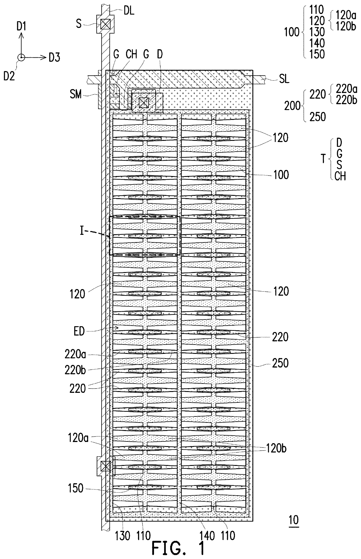
Figure 1 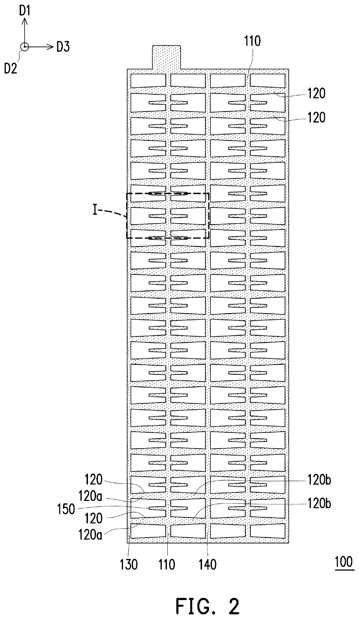
Figure 2 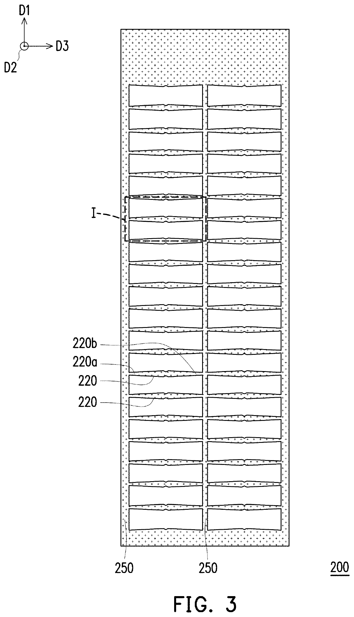
Figure 3
Abstract
Description
CROSS REFERENCE TO RELATED APPLICATION
[0001] This application claims the priority benefit of Taiwan application serial no. 107127445, filed on Aug. 7, 2018. The entirety of the above-mentioned patent application is hereby incorporated by reference herein and made a part of specification.BACKGROUND OF THE INVENTION1. Technical Field
[0002] The disclosure relates to a pixel structure, and more particularly to a pixel structure used in a display panel.2. Description of Related Art
[0003] As the size of the eSports market is becoming larger and larger, portable laptops specifically designed for eSports are one of key products that various electronics manufacturers have devoted to developing over the recent years. How to provide consumers with a portable eSports product with high performance, low energy consumption and high display quality is a vital challenge with which all the manufacturers are confronted, and a display panel with low energy consumption, high resolution, rapid response spee...
Examples
first embodiment
[0063]FIG. 7 is a cross-sectional view of a pixel structure according to the disclosure. Particularly, FIG. 7 is a cross-section of FIG. 4 taken along section line A-A′, and a film layer below the first electrode 100 of the pixel structure 10 is omitted from FIG. 7. Referring to FIGS. 1, 3 and 7, in the embodiment, the pixel structure 10 further includes a second electrode 200 disposed on the first electrode 100. In detail, the pixel structure 10 further includes a first insulating layer 300 disposed between the first electrode 100 and the second electrode 200. For example, the first insulating layer 300 may cover the first electrode 100, and the second electrode 200 is disposed on the first insulating layer 300. However, the disclosure is not limited to the embodiment. According to other embodiments, the first electrode 100 may also be disposed on the second electrode 200. One of the first electrode 100 and the second electrode 200 may serve as a pixel electrode, and the other of t...
second embodiment
[0089]FIG. 17 is an enlarged view of a display panel using the pixel structure 10A according to the disclosure driven by voltages. FIG. 18 is an enlarged view of a display panel using a pixel structure 33 according to the fourth comparative example of the disclosure driven by voltages. In particular, FIG. 17 illustrates that the pixel structure 10A is disposed between two polarizing plates having two transparent axes that are perpendicular to each other and shows the light penetration when voltages of 6 volts and 0 volt are applied to the first electrode 100-A and the second electrode 200-A of the pixel structure 10A respectively. In detail, the transparent axis of one of the polarizing plates that are perpendicular to each other is parallel to the first direction D1. FIG. 18 illustrates that the pixel structure 33 is disposed between polarizing plates having two transparent axes that are perpendicular to each other and shows the light penetration when voltages of 6 volts and 0 volt...
fifth embodiment
[0099]FIG. 27 is an enlarged front view of a display panel of a pixel structure 10D according to the disclosure. In particular, FIG. 27 illustrates that the pixel structure 10D is disposed between polarizing plates having two transparent axes that are perpendicular to each other and shows the light penetration when voltages of 6 volts and 0 volt are applied to a first electrode 100-D and a second electrode 200-D of the pixel structure 10D respectively. In detail, the transparent axis of one of the polarizing plates that are perpendicular to each other is parallel to the first direction D1.
[0100]Referring to FIGS. 26 and 27, the difference between the pixel structure 10D according to the embodiment and the pixel structure 10C according to the fourth embodiment is that a material of the first electrode 100-D according to the embodiment is a light-shielding conductive material such as metals or alloys. Compared with the pixel structure 10C according to the fourth embodiment, the first ...