
Backplane substrate and organic light emitting diode display using the same
a technology of organic light-emitting diodes and substrates, which is applied in the field of backplane substrates, can solve the problems of difficult to achieve realistic gradation expression on the screen, and difficulty in implementing devices having sufficient holding characteristics, and achieve the effect of sufficient storage capacitan
Patent Information
- Authority / Receiving Office
- US · United States
- Patent Type
- Patents(United States)
- Current Assignee / Owner
- Publication Date
- 2018-09-25
Smart Images
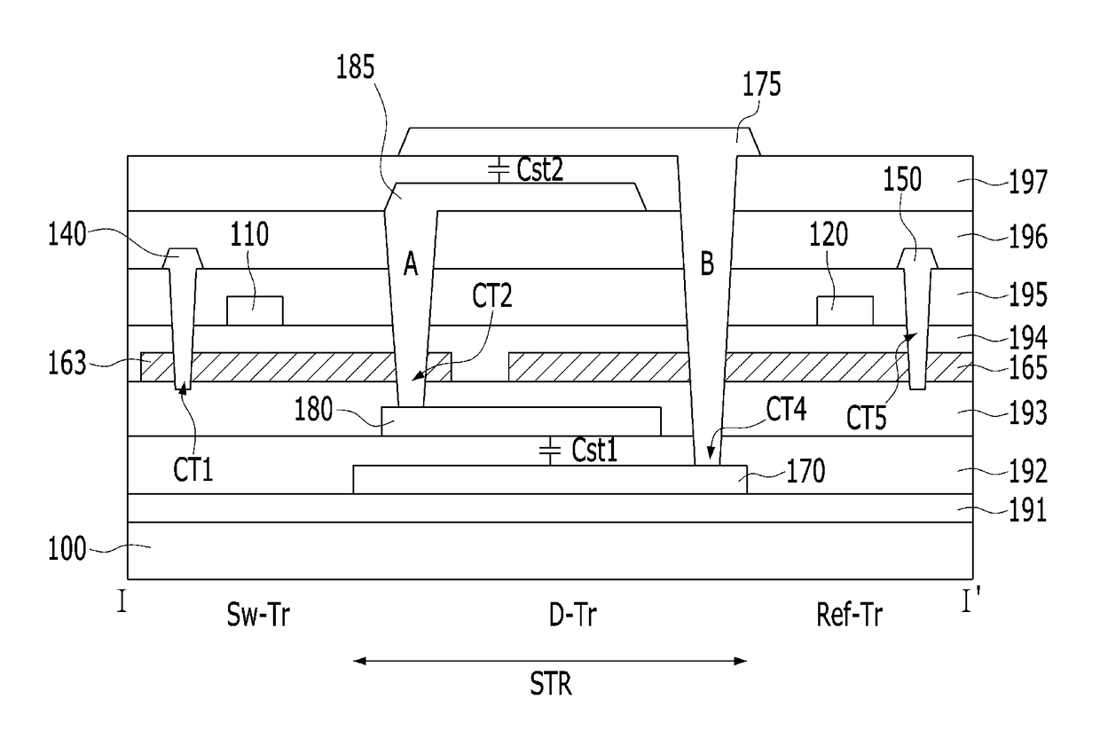
Figure 1 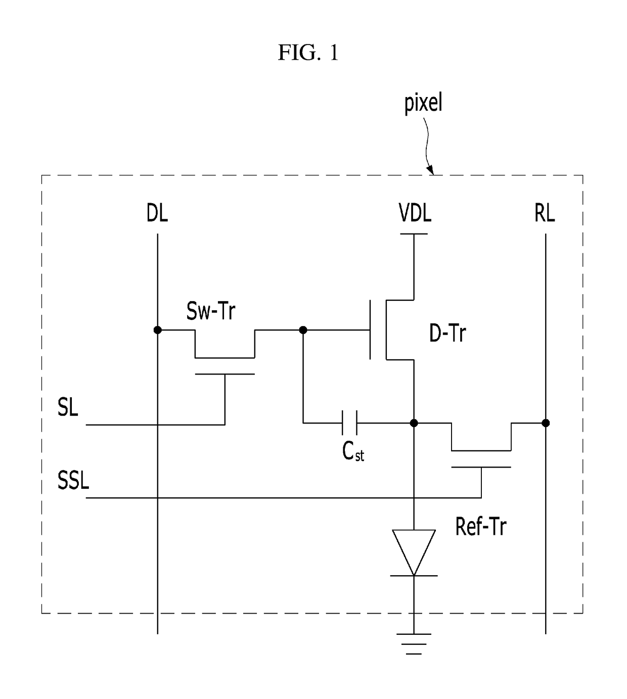
Figure 2 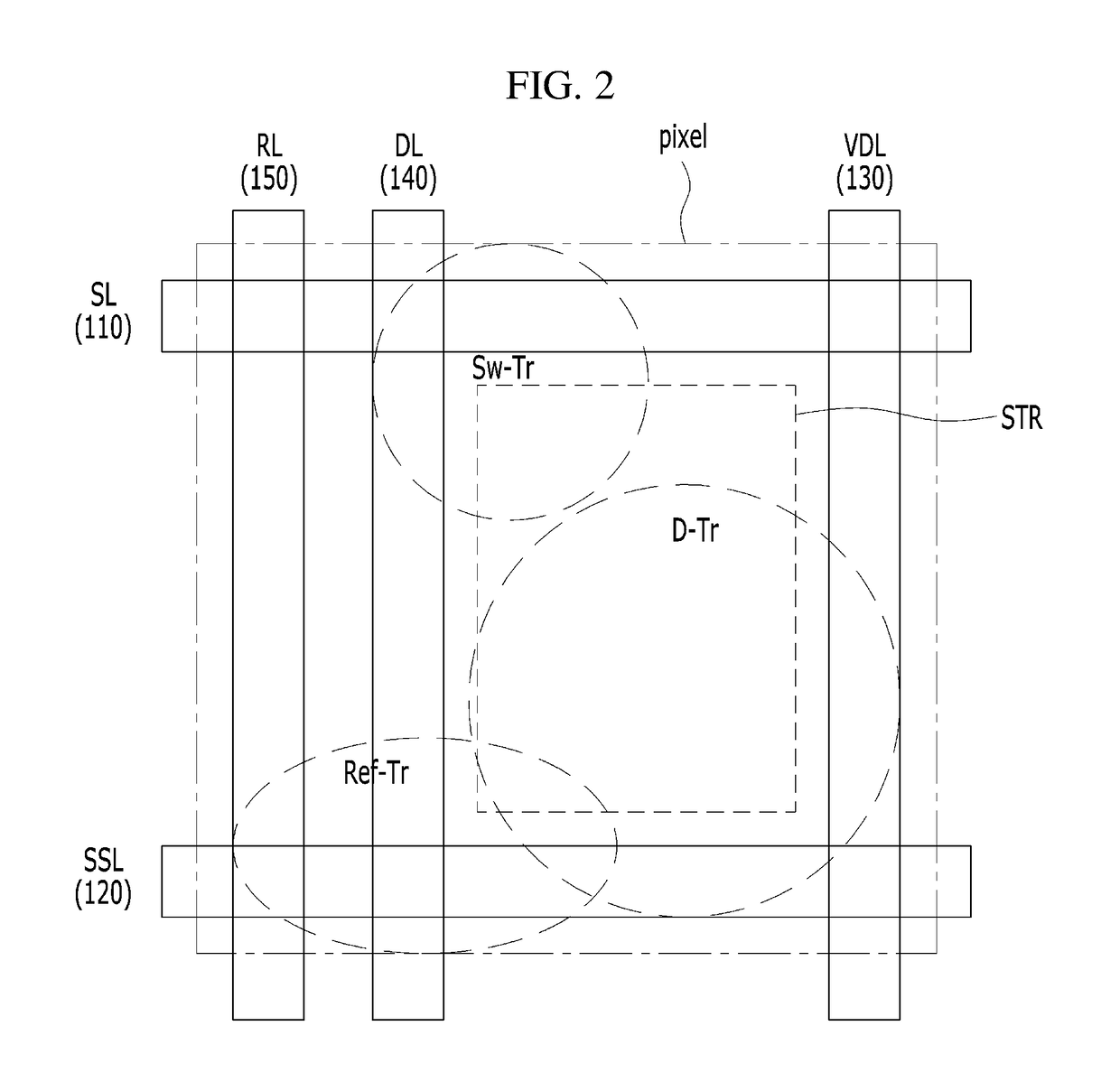
Figure 3
Abstract
Description
CROSS REFERENCE TO RELATED APPLICATIONS
[0001] This application claims the benefit of Korean Patent Applications Nos. 10-2016-0053476 filed on Apr. 29, 2016 and 10-2016-00127085 filed on Sep. 30, 2016, which are hereby incorporated by reference in their entirety.BACKGROUND OF THE DISCLOSUREField of the Disclosure
[0002] The present disclosure relates to a backplane substrate, and more particularly, to a backplane substrate which provides sufficient storage capacitance even when using small sub-pixels in a structure having a very high resolution, and an organic light emitting diode display using the same.Discussion of the Related Art
[0003] As various portable electronic devices, such as a mobile communication terminal, a notebook computer, etc., have been developed, requirements for flat panel display devices applied thereto have increased.
[0004] As representative examples of the flat panel display devices, liquid crystal displays (LCDs), plasma display panels (PDPs), field emission displa...
Examples
Embodiment Construction
[0044]Reference will now be made in detail to the aspects of the present disclosure, examples of which are illustrated in the accompanying drawings. Wherever possible, the same reference numbers will be used throughout the drawings to refer to the same or like parts. In the following description of the present disclosure, a detailed description of known functions and configurations incorporated herein will be omitted when it may make the subject matter of the present disclosure rather unclear. Also, the names of elements used in the following description are defined in consideration of ease in preparation of the specification and may differ from the names of elements of an actual product.
[0045]FIG. 1 is a circuit diagram of a sub-pixel of an organic light emitting diode display in accordance with the present disclosure, and FIG. 2 is a plan view illustrating a storage capacitor region within a sub-pixel region of FIG. 1.
[0046]Each sub-pixel of the organic light emitting diode displa...