
Liquid crystal display device
a liquid crystal display and display screen technology, applied in non-linear optics, instruments, optics, etc., can solve the problems of insufficient storage capacitance, inability to increase the aperture ratio, and inability to widen the range of driving liquid crystal molecules in the sub-pixel, so as to achieve sufficient storage capacitance. the effect of sufficient assuran
Patent Information
- Authority / Receiving Office
- US · United States
- Patent Type
- Patents(United States)
- Current Assignee / Owner
- Publication Date
- 2016-07-12
Smart Images
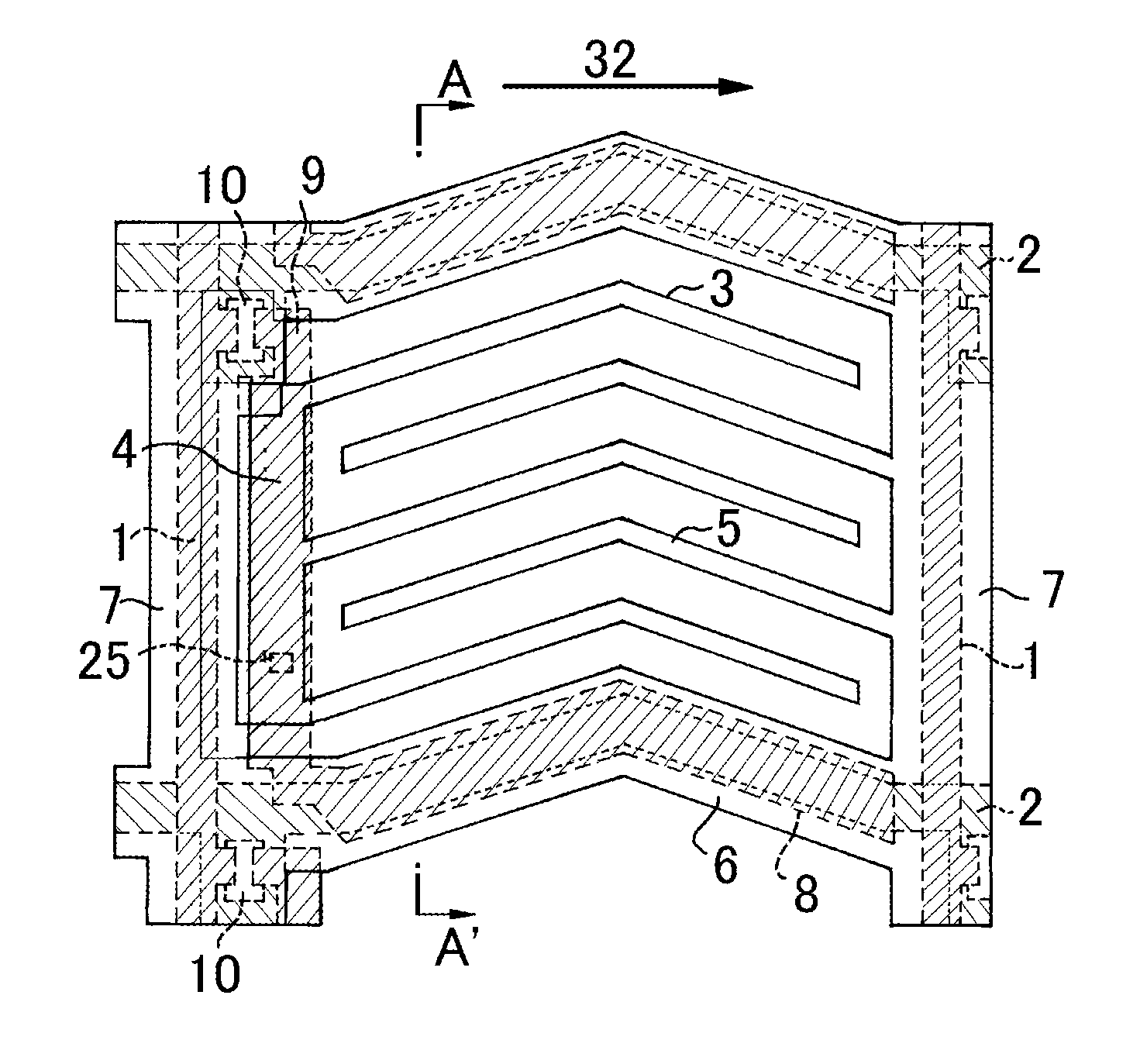
Figure 1 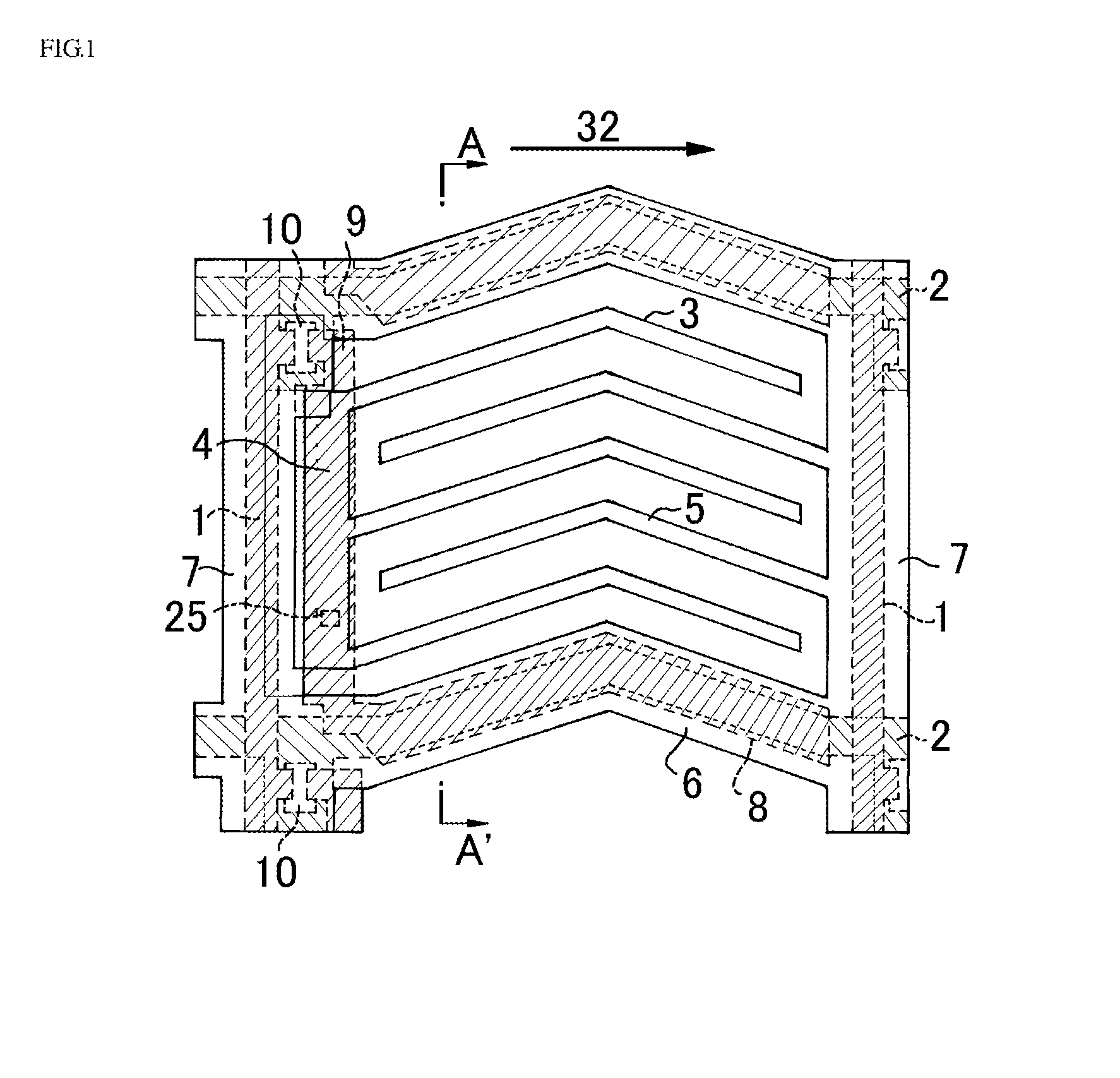
Figure 2 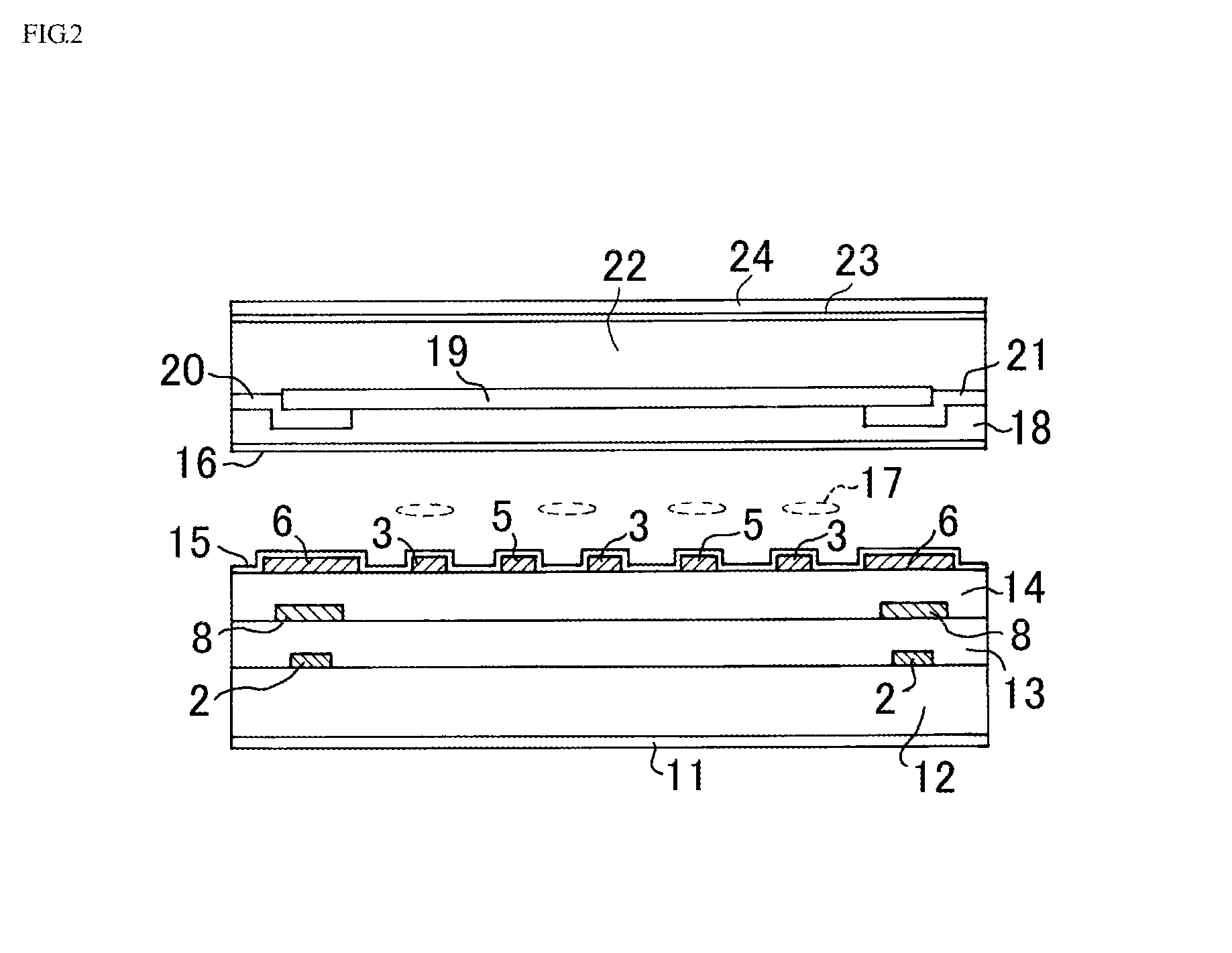
Figure 3
Abstract
Description
TECHNICAL FIELD
[0001] The present invention relates to a liquid crystal display device and, more particularly, to an active-matrix-type liquid crystal display device in which liquid crystal molecules are driven with an electric field substantially perpendicular to a thin film transistor substrate.BACKGROUND ART
[0002] A liquid crystal display device of a TN (Twisted Nematic) type being widely used has high contrast but, on the other hand, has a problem of high visual angle dependence since the molecular axis of the liquid crystal rises due to the vertical electric field. Since demand for a large-sized monitor of a TV or the like is increasing in recent years, a so-called transverse-electric-field-type liquid crystal panel such as the IPS (In-Plane Switching) type or FFS type is being spread, in which an electric field substantially parallel to a substrate for which thin film transistors (hereinafter, called TFTs) are provided is applied to liquid crystal molecules to drive the molecule...
Examples
first embodiment
[0023]As illustrated in FIG. 1, in a liquid crystal display device, a plurality of data lines 1 are disposed in parallel to one another on a transparent substrate (first substrate). A plurality of scan lines 2 are disposed substantially perpendicular to the data lines 1. By the plurality of data lines 1 and the scan lines 2, a plurality of sub pixel regions arranged in a matrix are defined.
[0024]A gate electrode is provided on the scan line 2 near a part crossing the data line 1, and the drain electrode is connected from the data line 1 crossing the scan line 2. With such a structure, a thin film transistor can be formed near the crossing part of the data line 1 and the scan line 2.
[0025]On one of the sides of the data line 1, a source pixel electrode (an electric potential supply line connected to the source electrode) is disposed along the data line 1, and the source electrode of the TFT is connected to the source pixel electrode
[0026]Pixel electrodes are disposed in a layer upper...
second embodiment
[0057]A second embodiment of the present invention will be described with reference to FIGS. 5 and 6. FIG. 5 is a plan view illustrating the configuration of one sub pixel in a liquid crystal display device as a second embodiment of the present invention. FIG. 6 is a cross section taken along line A-A′ of FIG. 5.
[0058]The pixel of the second embodiment illustrated in FIGS. 5 and 6 will be described in detail in fabricating order.
[0059]First, on a glass substrate as the first insulating substrate 12, the scan line 2 is formed by a first metal layer made by 2500 A of Cr.
[0060]As the gate insulating film 13, 5000 A of SiNx and a thin film semiconductor layer made of 2000 A of a-Si and 500 A of n-a-Si are formed. The thin film semiconductor layer 10 is patterned while leaving only a TFT part provided as a switching element of the pixel. By a second metal layer made by 2500 A of Cr, the data line 1, source / drain electrodes of the TFT, the source pixel electrode 9 connected to the source ...
third embodiment
[0083]A third embodiment of the present invention will be described with reference to FIGS. 7, 8, and 9. FIG. 7 is a plan view illustrating the configuration of one sub pixel in a liquid crystal display device as a third embodiment of the present invention. FIG. 8 is a cross section of a TFT substrate, taken along line A-A′ in FIG. 7.
[0084]The pixel of the second embodiment illustrated in FIGS. 7 to 9 will be described in detail in fabricating order.
[0085]First, on a glass substrate as the first insulating substrate 12, the scan line 2 is formed by a first metal layer made by 2500 A of Cr.
[0086]As the gate insulating film 13, 5000 A of SiNx and a thin film semiconductor layer made of 2000 A of a-Si and 500 A of n-a-Si are formed. The thin film semiconductor layer 10 is patterned while leaving only a TFT part provided as a switching element of the pixel. By a second metal layer made by 2500 A of Cr, the data line 1, source / drain electrodes of the TFT, the source pixel electrode 9 con...