
Active matrix type liquid crystal display device
Patent Information
- Authority / Receiving Office
- US · United States
- Current Assignee / Owner
- Publication Date
- 2007-08-23
- Estimated Expiration
- Not applicable · inactive patent
Smart Images
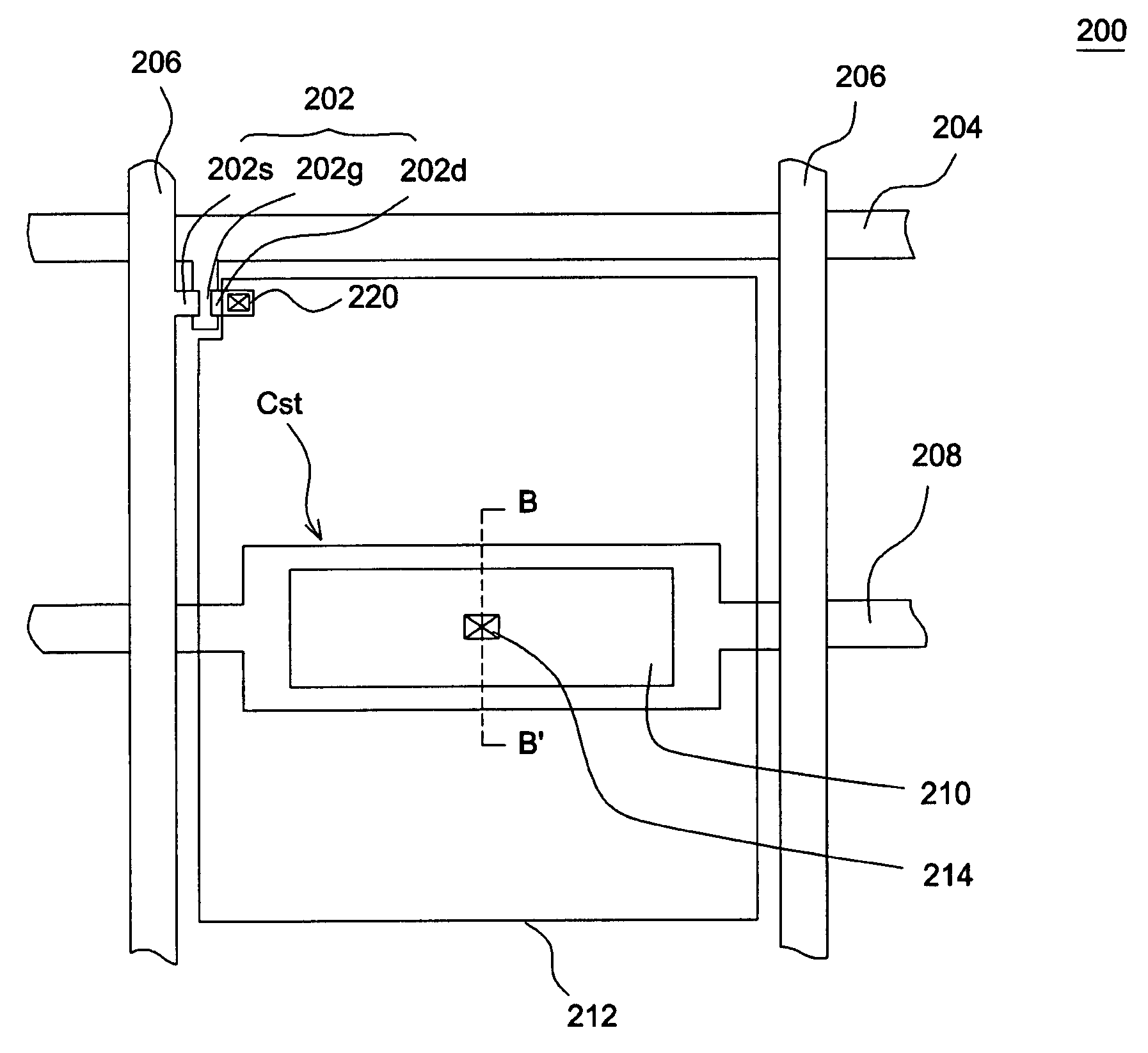
Figure 1 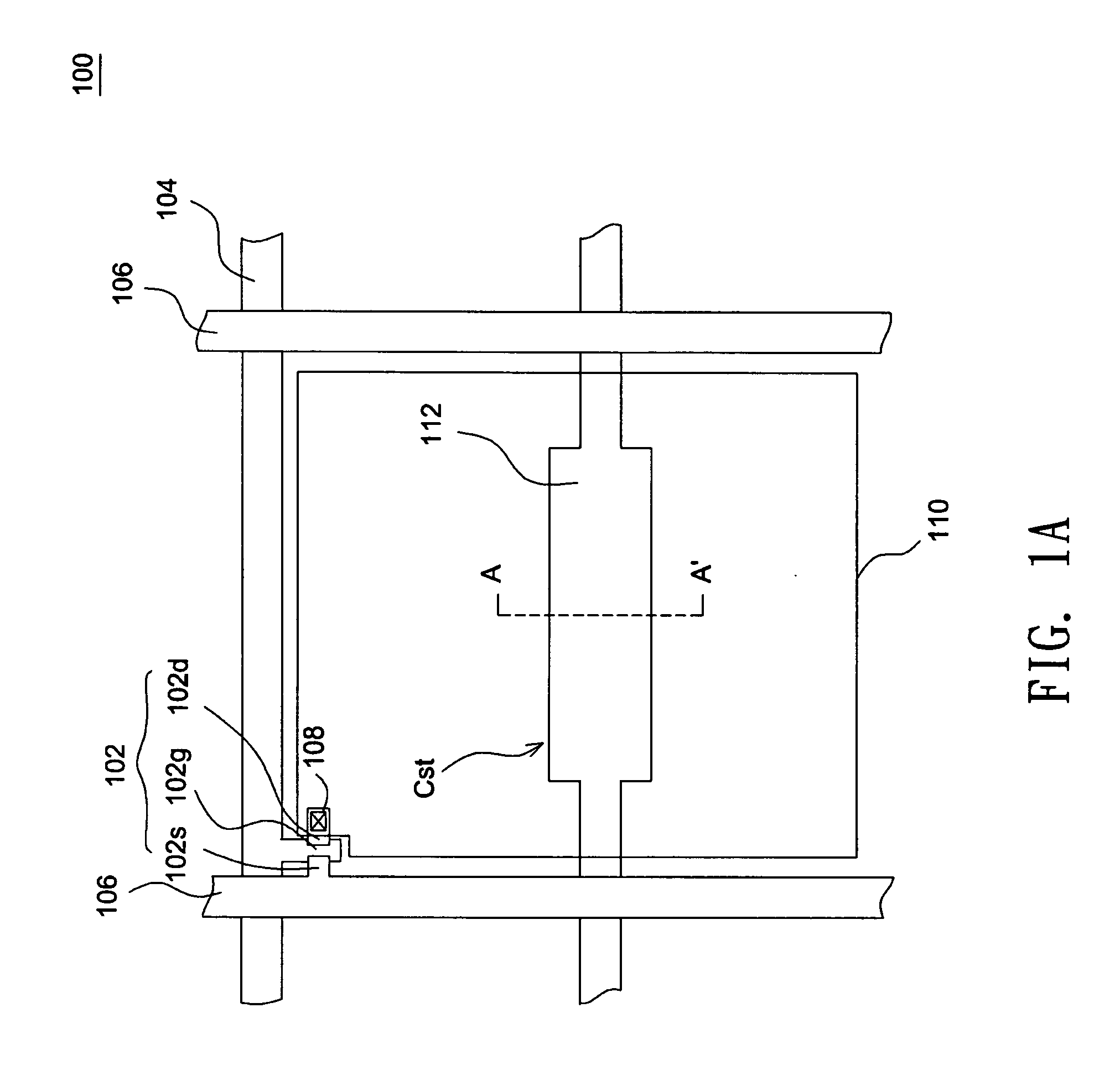
Figure 2 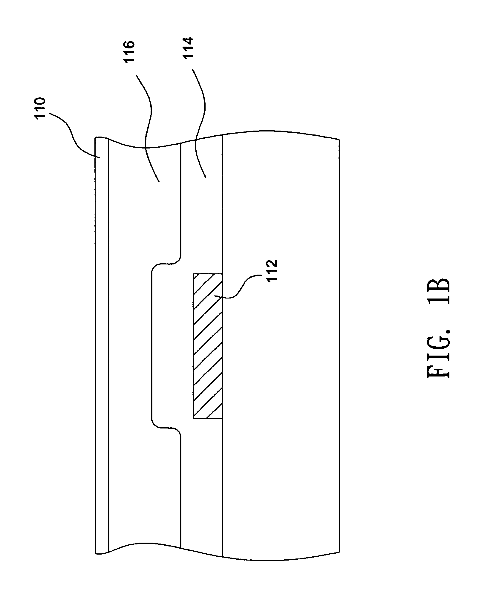
Figure 3
Abstract
Description
CROSS REFERENCE TO RELATED PATENT APPLICATION
[0001] The present application claims priority under 35 U.S.C. §119(a) on Patent Application No. 095104149 filed in Taiwan on Feb. 8, 2006, the entire contents of which are hereby incorporated by reference.BACKGROUND OF THE INVENTION
[0002] (a) Field of the Invention
[0003] The invention relates to an active matrix type liquid crystal display (AM LCD) device having a high aperture ratio.
[0004] (b) Description of the Related Art
[0005] At present, the dominant method for fabricating an active matrix liquid crystal display device is typically based on amorphous silicon thin film transistor (a-Si TFT) technologies.
[0006] FIG. 1A shows a plan view illustrating a conventional active matrix display device 100. FIG. 1B shows a cross-sectional view of the active matrix display device shown in FIG. 1A, taken along line A-A′. Referring to FIG. 1A, the gate 102g of an n-type a-Si TFT 102 is connected to a gate line 106, its source 102s is connected to a data...
Examples
Embodiment Construction
[0018]FIG. 3 shows a partial cross-sectional view illustrating an active matrix type liquid crystal display (AM LCD) device 10 according to the invention. Referring to FIG. 3, the display device 10 includes a color filter substrate 12 and an array substrate 14, with a liquid crystal layer 16 interposed between them. In the array substrate 14, a switching device such as a thin film transistor (TFT) 18, a pixel electrode 22, and a first alignment layer 24 are formed on a transparent substrate 15. Further, in the color filter substrate 12, a color filter 26, a black matrix layer 28, a common electrode 32, and a second alignment layer 34 are formed on a transparent substrate 13.
[0019]FIGS. 4A and 4B show schematic diagrams illustrating an embodiment of a pixel structure 40 of an active matrix display device according to the invention, where FIG. 4A shows a plan view observed from the normal direction of an array substrate, and FIG. 4B shows a cross-sectional view taken along line C-C′ i...