
Pixel structure and fabrication method of pixel structure
a technology of pixel structure and fabrication method, which is applied in the direction of optics, transistors, instruments, etc., can solve the problems of inability to characterize the existing pixel structure, further limit the display aperture ratio, etc., and achieve the effect of increasing the display aperture ratio and sufficient storage capacitan
Patent Information
- Authority / Receiving Office
- US · United States
- Patent Type
- Patents(United States)
- Current Assignee / Owner
- Publication Date
- 2013-11-12
Smart Images
Figure 1 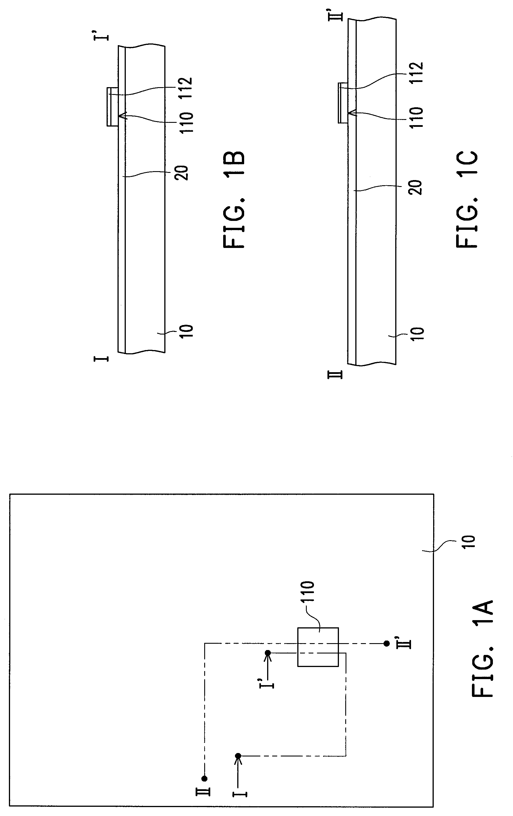
Figure 2 
Figure 3
Abstract
Description
CROSS-REFERENCE TO RELATED APPLICATION
[0001] This application claims the priority benefit of Taiwan application serial no. 100141606, filed on Nov. 15, 2011. The entirety of the above-mentioned patent application is hereby incorporated by reference herein and made a part of this specification.BACKGROUND OF THE INVENTION
[0002] 1. Field of the Invention
[0003] The invention relates to a pixel structure and a fabrication method of the pixel structure. More particularly, the invention relates to both a pixel structure that has a high aperture ratio and can be easily fabricated and a fabrication method of the pixel structure.
[0004] 2. Description of Related Art
[0005] In general, a pixel structure of a liquid crystal display (LCD) includes active devices and pixel electrodes. The active devices serve as switches of LCD display units. To control each pixel structure, a certain pixel is usually selected by a corresponding scan line and a corresponding data line, and display information correspond...
Examples
Embodiment Construction
[0038]FIG. 1A is a schematic top view illustrating a fabrication method of a pixel structure with use of a first photomask according to an embodiment of the invention. FIG. 1B and FIG. 1C are respectively cross-sectional views taken along section lines I-I′ and II-II′ depicted in FIG. 1A. With reference to FIG. 1A, FIG. 1B, and FIG. 1C, in the fabrication method described in the present embodiment, a channel layer 110 is formed on a substrate 10. The channel layer 110 may be formed with use of the first photomask. Namely, in this step, a layer of semiconductor material is formed on the substrate 10 by performing a physical vapor deposition (PVD) process, a chemical vapor deposition (CVD) process, a sputtering process, or the like deposition process. A photolithography and an etching processes are performed with use of a first photomask (not shown), so as to pattern the layer of semiconductor material and to form the channel layer 110.
[0039]According to the present embodiment of the ...