
Manufacturing method of display panel
a manufacturing method and display panel technology, applied in the field of manufacturing methods of display panels, can solve the problems of increasing manufacturing costs, and achieve the effect of increasing storage capacitance and good electrical properties
Patent Information
- Authority / Receiving Office
- US · United States
- Patent Type
- Patents(United States)
- Current Assignee / Owner
- Publication Date
- 2021-10-19
Smart Images
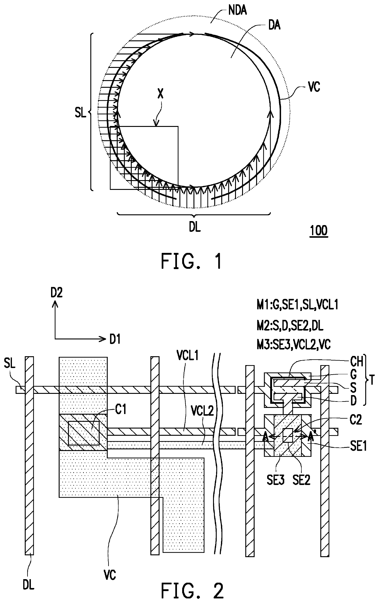
Figure 1 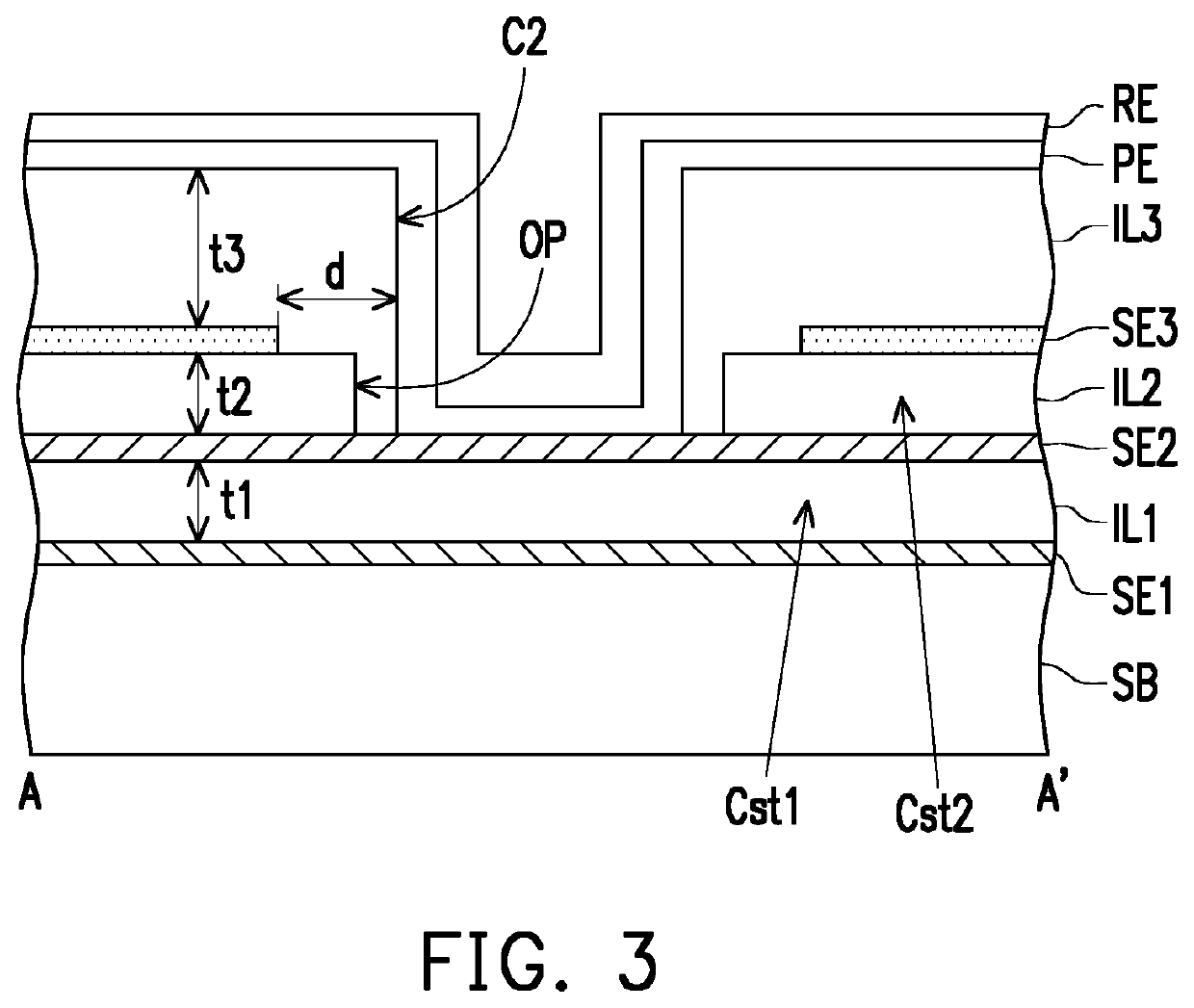
Figure 2 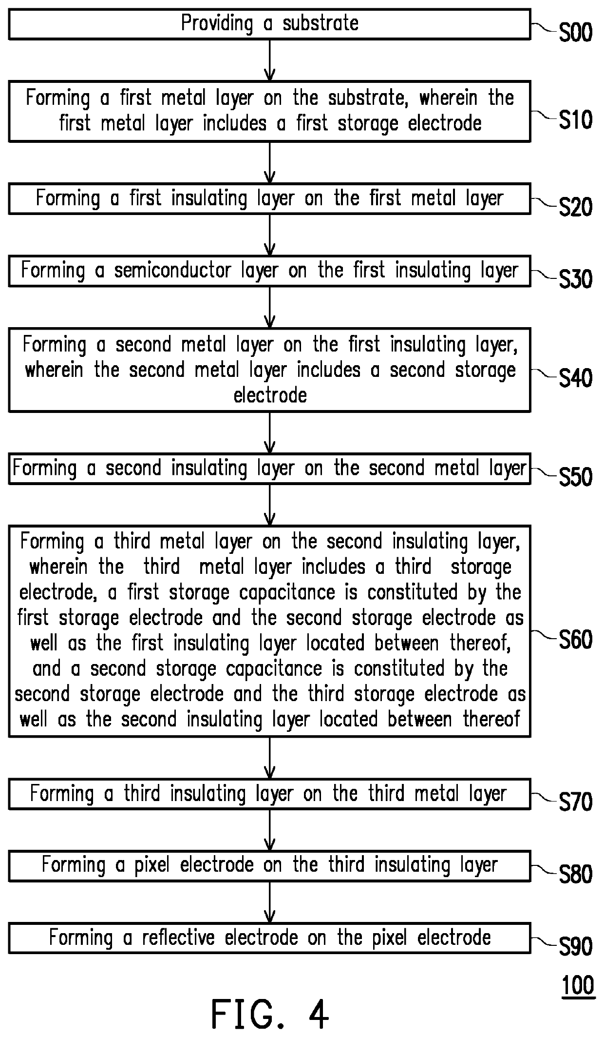
Figure 3
Abstract
Description
CROSS-REFERENCE TO RELATED APPLICATION
[0001] This application claims the priority benefit of Taiwan application serial no. 109131890, filed on Sep. 16, 2020. The entirety of the above-mentioned patent application is hereby incorporated by reference herein and made a part of this specification.BACKGROUNDTechnical Field
[0002] The disclosure is related to a manufacturing method of a display panel, and particularly to a manufacturing method of a display panel with increased storage capacitance.Description of Related Art
[0003] Referring to FIG. 5, a scan line 20 is a portion of a first metal layer and a data line 30 is a portion of a second metal layer in a non-rectangular (such as circular) display panel 10, wherein the data line 30 is located above the scan line 20. A portion of a common voltage line located in a non-display area 10b of the prior art, surrounding a display area 10a, would be connected to the data line 30 to generate the short circuit since the common voltage line of the p...
Examples
Embodiment Construction
[0020]The disclosure is more comprehensively described with reference to the figures of the present embodiments. However, the disclosure may also be implemented in various different forms, and is not limited to the embodiments in the present specification. The thicknesses of the layers and regions in the figures are enlarged for clarity. The same or similar reference numerals represent the same or similar devices and are not repeated in the following paragraphs. Additionally, directional terminology, such as “top,”“bottom,”“left,”“right,”“front,” or “back,” etc., is used with reference to the orientation of the Figure(s) being described. As such, the directional terminology is used for purposes of illustration and is in no way limiting.
[0021]FIG. 1 is a schematic top view of a display panel according to one embodiment of the disclosure, FIG. 2 is an enlarged schematic top view of region X in FIG. 1, FIG. 3 is a schematic cross-sectional view taken along a sectional line A-A′ depicte...